
A Dual ADC/DAC using the Red Pitaya Board
The Red Pitaya boards provide a convenient and cost effective method for spanning the analog/digital divide when prototyping RF systems. Provision is made on the rfblocks module carrier boards for mounting a Red Pitaya board. This document describes a dual channel ADC/DAC design specifically for use with the rfblocks ecosystem.
Base Band Signal Acquisition
Figure 1 shows a diagram of the essential components when using the Red Pitaya board within the rfblocks framework.

Figure 1: Dual ADC base band context
Figures 2a and 2b show the physical connections required in order to use the Red Pitaya based dual DAC/ADC to acquire base band signals for processing in the digital domain.
RF signal inputs are connected at the front of the enclosure as shown in Figure 2a. Connections for the Red Pitaya board are made at the rear of the enclosure as shown in Figure 2b. Power for the step attenuators and optional amplifiers (if fitted) is also connected at the rear of the enclosure (the 12-15VDC barrel connector).
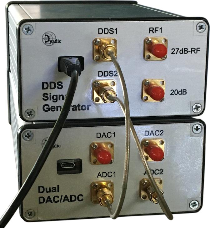
Figure 2a: Dual DAC/ADC connected to acquire input from a DDS signal generator.
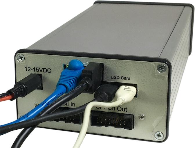
Figure 2b: Dual DAC/ADC rear connections
Hardware Design

Figure 3: Base band front end schematic

Figure 4: Red Pitaya SDRlab 122-16 ADC input/DAC output networks.
The ADC input signal chain consists of a PE43711 based step attenuator followed by an anti-alias filter based on the Minicircuits RLP-40 filter. Provision is also made for an amplifer module which can be used to increase the low power dynamic range (the GRF4014 10-300 MHz gain block design has been used in this capacity).
The Red Pitaya Zynq SPI and GPIO facilities are used to directly control the step attenuators.
The design also includes a microcontroller (in this case an atmega32 USB controller). SPI and GPIO lines from this controller are connected directly to the SPI control output connector at the rear of the enclosure. This allows for the control of external designs such as the dual RF down converter (which does not have an integral controller).
A rough measurement of the noise figure was made using the following technique:
A low noise pre-amplifier is connected to the RF input of the selected channel. In this case the GRF4014 (10-300MHz tune) is used. This has a noise figure of about 2.5 dB with a gain of about 29 dB at 30 MHz.
The noise figure is measured using the Y-factor method with the RF Gadgets XDM-1600 noise source. The noise measurement is made at base band with a full span (54.5 MHz). Measured power levels with the noise source off and on respectively are: -90.3 dBm and -77.4 dBm. This gives a noise figure of approximately 2.65 dB.

Figure 5: Red Pitaya board top showing GPIO pins in expansion connectors

Figure 6a: E1 Expansion Connection pinout

Figure 6b: E2 Expansion Connector pinout
Design Notes
Intermodulation
Direct measurement of third order IMD indicates < -115 dBm with a two tone separation of 2 MHz and fundamental power of approximately -10 dBm. This corresponds to an IP3 of better than 42 dBm.

Figure 5: Red Pitaya SDRlab 122-16 ADC base band IM3.

Figure 6: ADC base band IM3 test setup.
The IM3 test setup consisted of a dual channel DDS signal generator with output from the two channels combined using a resistive bridge coupler. The two DDS channels were tuned for a separation of 2 MHz with the lower frequency tone at 31.27 MHz and the upper tone at 33.27 MHz. These frequencies were chosen to avoid the worst of the DDS spurs.
Noise
The measured DANL for the base band design is -144.6 dBm/Hz. This corresponds to a noise figure of 29.4 dB.
Assembly
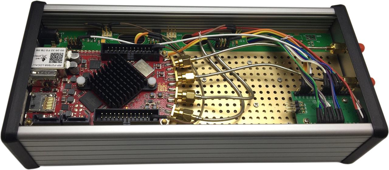
Figure 5a: Top side of assembly.
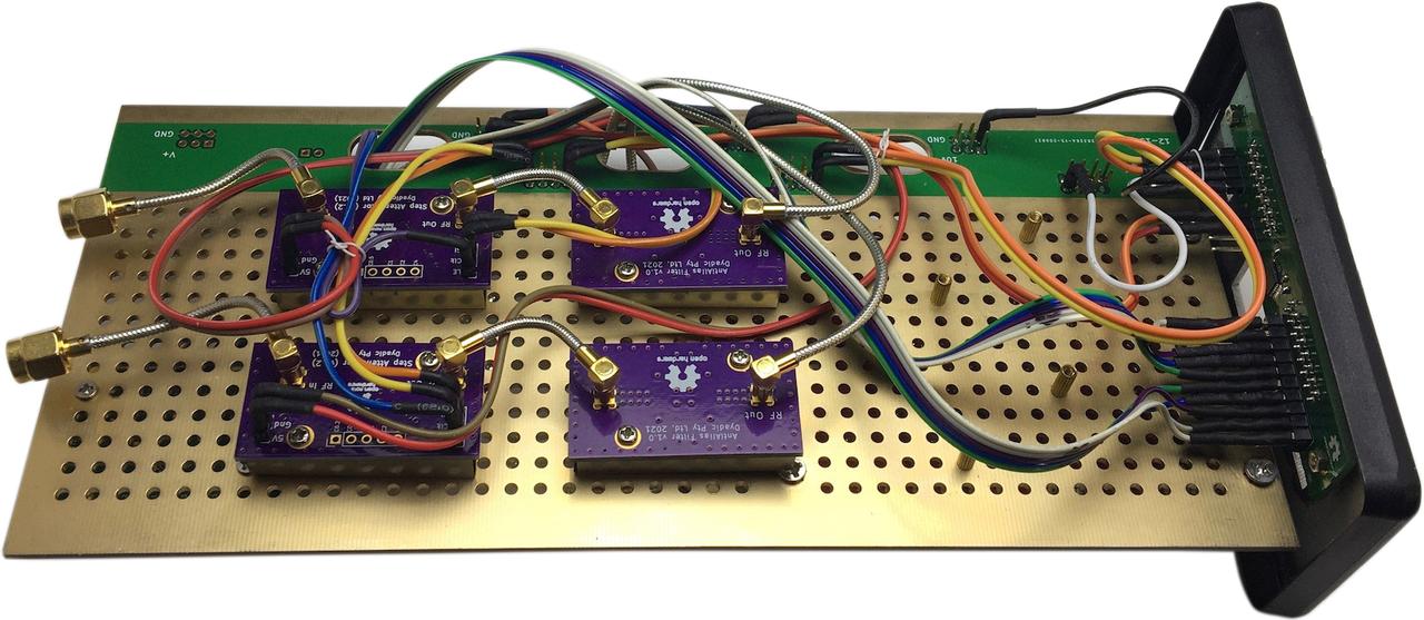
Figure 5b: Reverse side of assembly.
The rfblocks module carrier boards are designed to accept Red Pitaya boards at the rear next to the input power connector. Figure 4a shows the Red Pitaya board mounted on the top side of the module carrier. The DAC outputs are connected directly to the enclosure SMA outputs. External RF inputs are taken through the enclosure SMA inputs to the step attenuators and then the anti-alias filters, mounted on the reverse side of the module carrier board (Figure 5b). Outputs of the anti-alias filters are then connected directly to the Red Pitaya board ADC inputs. There is also provision for the installation of amplifier modules for increasing the low power dynamic range.
Figure 2b shows the connections to the Red Pitaya board at the rear of the enclosure. These are, from let to right, Ethernet, USB hub connection, USB/Serial console connection, and USB power connection.
Software Environment
The software environment consist of the following on the Red Pitaya board:
The base operating system
Optionally, a TCP to serial bridge instance
And the following on the client host(s);
Client application - for example Red Pitaya Spectrum Analyzer.
Optionally, one or more TCP to serial bridge instances.
Optionally, one or more rfblocks application launchers.
ADC DMA Zynq Programmable Logic
The Zynq programmable logic design makes use of Pavel Demin's library of cores for the Xilinx Vivado/Vitis tools. At the top level, the AXI4-Stream Red Pitaya ADC is used to provide a stream of data from the two on board ADC channels. A copy of this stream is sent to DMA unit which presents the stream as 'raw' ADC samples.
Another copy is sent to a broadcast core which splits the ADC stream into two more streams each containing the data from one of the ADC channels. These streams are then sent to digital down conversion (DDC) modules. The output of the DDC modules are presented to two DMA units - one for each ADC channel. The DDC modules are configured via a configuration register core.
The vivado block design file is available here: ADC block design.

Figure 6: Red Pitaya ADC DMA top level design
The DDC cores implement the following functions:
Correct the input sample data for any DC offset.
Optionally shift the base band spectrum using a combination of DDS NCO and complex multiplier to form a mixer with a configurable local oscillator. The output from the multiplier is the shifted base band represented as I/Q (inphase/quadrature) sample data.
Optionally decimate the base band samples. A combination of a CIC filter followed by a FIR compensation filter used to flatten the CIC pass band frequency response. A stream switch allows either the decimated sample stream or the full rate sample stream to be selected as the output from the core.
The DDC core configuration registers are accessed via a Linux userspace I/O (UIO) device. The switch configuration is also accessed as a register via a separate UIO device.
The DDC core block design file is available here: ddc.tcl.

Figure 7: Red Pitaya ADC DMA down converter design
DDC sample rate conversion filtering
FIR filter coefficients are calculated using the following script. Note
that the stop band rejection and window transition width are both
hardcoded to be 75 dB (rej) and 0.07 (width, in Nyquist units). The
default values for the CIC decimator are order (N) 6, and differential
delay (M) of 2.

Figure 8: Combined CIC and FIR compensation filter response.
import sys
from argparse import ArgumentParser
import numpy as np
from scipy import signal
import matplotlib.pyplot as plt
from dyadic.splot import init_style


if __name__ == '__main__':

    N = 6  # Default stages
    R = 8  # Default decimation rate
    M = 2  # Default differential delay
    Fo = 0.15  # Default cutoff freq. (Nyquist units)

    parser = ArgumentParser(
        description='Generate coefficients for a FIR filter to '
        + 'compensate for a CIC decimator frequency response.'
    )

    parser.add_argument(
        "-S", "--stages", default=N, type=int,
        help=f"The number of CIC decimator stages. Default: {N}"
    )
    parser.add_argument(
        "-R", "--rate", default=R, type=int,
        help=f"The CIC decimator decimation factor. Default: {R}"
    )
    parser.add_argument(
        "-D", "--ddelay", default=M, type=int,
        help=f"The CIC decimator differential delay. Default: {M}"
    )
    parser.add_argument(
        "-C", "--cutoff", default=Fo, type=float,
        help=f"The filter cutoff frequency in Nyquist units. Default: {Fo}"
    )
    args = parser.parse_args()

    # Use a stop band rejection of 75dB.
    rej = 75.0

    # Window transition width
    width = 0.07

    M = args.ddelay
    R = args.rate

    # Calculate FIR window parameters
    (numtaps, beta) = signal.kaiserord(rej, width)

    # Calculate frequency and gain arrays
    p = 2e3
    s = 0.25/p
    fp = np.append(np.arange(0, args.cutoff, s), args.cutoff)
    fs = np.arange(args.cutoff+s, 0.5, s)
    f = np.concatenate((fp, fs)) * 2
    Mp = np.ones(len(fp))
    Mp[1:] = np.abs(M*R*np.sin(np.pi*fp[1:]/R)/np.sin(np.pi*M*fp[1:]))**N
    Mf = np.concatenate((Mp, np.zeros(len(fs))))
    f[-1] = 1.0

    h = signal.firwin2(numtaps, f, Mf, window=('kaiser', beta))
    h = h / np.sum(h)
    print(f'Filter coefficients ({numtaps=}):')
    print(', '.join(f'{f:.10g}' for f in h))

    w, Mactual = signal.freqz(h, worN=2048)
    init_style()
    fig = plt.figure(num=None, figsize=(8.0, 6.0), dpi=72)
    ax = fig.add_subplot(121)
    _ = ax.set_xlabel('Normalized frequency')
    _ = ax.set_ylabel('Filter gain')
    _ = ax.set_xlim(0.0, 0.5)
    ax.plot(w/np.pi, np.abs(Mactual))
    ax.plot(f, Mf)

    ax = fig.add_subplot(122)
    _ = ax.set_xlabel('Normalized frequency')
    _ = ax.set_ylabel('Filter gain (dB)')
    _ = ax.set_xlim(0.0, 0.5)
    ax.plot(w/np.pi, 20*np.log10(np.abs(Mactual)))
    ax.plot(f, 20*np.log10(Mf+1e-5))
    fig.tight_layout()
    fig.show()

    input('Press any key to terminate> ')
When the output width is equal to the maximum register width, the core outputs the full precision result and the magnitude of the core output reflects the filter gain. When the output width is set to less than the maximum register width, the output is truncated with a corresponding reduction in gain.
When the core is configured to have a programmable rate change, there is a corresponding change in gain as the filter rate is changed. When the output is specified to full precision, the change in gain is apparent in the core output magnitude as the rate is changed. When the output is truncated, the core shifts the internal result, given the Bmax for the current rate change, to fully occupy the output bits.
ADC DMA and Buffering
The cma boot command line parameter is set to 132M. This allows for a
maximum either one 128MB channel buffer or two 64MB channel buffers.
bootargs=console=ttyPS0,115200 root=/dev/mmcblk0p2 ro rootfstype=ext4 earlyprintk cma=132M uio_pdrv_genirq.of_id=generic-uio rootwait
At the full sampling rate of 122.88 MSamples and a window size of 1000 this allows a resolution of about 8uS for about 65 mS with a 128MB buffer size.
DAC Zynq Programmable Logic

Figure 9: Red Pitaya DAC top level design
The vivado block design file is available here: DAC block design.

Figure 10: Red Pitaya DAC channel design