A PE4140B Quad FET Mixer
Features
Good broadband performance. 100 to 4000 MHz for both up- and down-conversion.
High linearity: nominal IIP3 of 30 dBm.
Nominal conversion loss of 6.5 dB.
Nominal 35 dB LO to RF isolation between 500 and 2000 MHz
Hardware Configurations
Design |
Board Variant |
LO Balun |
RF Balun |
IF Balun |
LO Amp. |
|---|---|---|---|---|---|
4:1 |
Standard |
TCM4-452X |
TCM4-452X |
ETC1-1-13TR |
GRF2013, 50-3000 MHz tune |
1:1-hifreq |
High Freq. |
TCM4-452X |
MABA-011082 |
WBC1-1TL |
GRF2013, 50-3000 MHz tune |
1:4-hifreq |
High Freq. |
TCM4-452X |
MABA-011082 |
WBC4-1WL |
GRF2013, 50-3000 MHz tune |
1:4 |
Standard |
TCM4-452X |
ETC1-1-13TR |
WBC4-6TL |
GRF2013, 50-3000 MHz tune |
Standard board variant
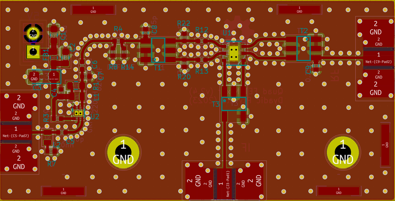
Figure 1a: Mixer module with LO amplifier and standard balun configuration
Figure 1b: Mixer module schematic design
High frequency board variant

Figure 2a: Mixer module with LO amplifier and high frequency balun configuration
Figure 2b: Mixer module schematic design
Typical Performance Characteristics
IIP3 and Conversion Loss
Design: 1:4-hifreq. High frequency board variant populated with TCM4-452X LO balun, MABA-011082 RF balun and WBC4-1WL IF balun. The LO amp. is GF2013 with the 50-3000 MHz tune. IMD measurements are taken with input 2-tone amplitude of -10 dBm and tone separation of 2 MHz. Loss measurements using input tone amplitude of -10 dBm. IF frequency is 30 MHz.
LO drive is adjusted to give optimal mixer IIP3:
Design: 1:1-hifreq. High frequency board variant populated with TCM4-452X LO balun, MABA-011082 RF balun and WBC1-1TL IF balun. The LO amp. is GF2013 with the 50-3000 MHz tune. IMD measurements are taken with input 2-tone amplitude of -10 dBm and tone separation of 2 MHz. Loss measurements using input tone amplitude of -10 dBm. IF frequency is 30 MHz.
LO drive is adjusted to give optimal mixer IIP3:
Design: 4:1. Standard board variant populated with TCM4-452X LO balun, TCM4-452X RF balun and ETC1-1-13TR IF balun. The LO amp. is GF2013 with the 50-3000 MHz tune. IMD measurements are taken with input 2-tone amplitude of -10 dBm and tone separation of 2 MHz. Loss measurements using input tone amplitude of -10 dBm. IF frequency is 30 MHz.
LO drive is adjusted to give optimal mixer IIP3:
Design: 1:4. Standard board variant populated with TCM4-452X LO balun, ETC1-1-13TR RF balun and WBC4-6TL IF balun. The LO amp. is GF2013 with the 50-3000 MHz tune. IMD measurements are taken with input 2-tone amplitude of -10 dBm and tone separation of 2 MHz. Loss measurements using input tone amplitude of -10 dBm. IF frequency is 30 MHz.
LO drive is adjusted to give optimal mixer IIP3:
Isolation
Spurious output levels
Spur measurements for mixer module with RF: TCM4-452X, LO: ETC1.6-4-2-3, IF: WBC1-1TL operating in up conversion mode
N |
||||||
|---|---|---|---|---|---|---|
1 |
2 |
3 |
4 |
5 |
||
0 |
-36 |
-19 |
-25 |
-30 |
-31 |
|
1 |
-22 |
-45 |
-40 |
-46 |
-52 |
|
M |
2 |
-70 |
-95 |
-87 |
-91 |
-96 |
3 |
-92 |
* |
* |
* |
* |
|
4 |
* |
* |
* |
* |
* |
|
5 |
* |
* |
* |
* |
* |
N |
||||||
|---|---|---|---|---|---|---|
1 |
2 |
3 |
4 |
5 |
||
0 |
-41 |
-25 |
-33 |
-26 |
-29 |
|
1 |
-22 |
-46 |
-34 |
-45 |
-37 |
|
M |
2 |
-69 |
-93 |
-83 |
-89 |
-85 |
3 |
-95 |
* |
* |
* |
-97 |
|
4 |
* |
* |
* |
* |
* |
|
5 |
* |
* |
* |
* |
* |
Spur measurements for mixer module with RF: TCM4-452X, LO: TCM4-452X, IF: ETC1-1-13 operating in up conversion mode
Applications Information
Reference Designs
Design Notes
Figure 1: Mixer schematic design.
Theoretical Background
The material in this section is based on an application note by Oxner and originally produced by Siliconix. A copy of the application note may still be available here: A Commutation Double-Balanced MOSFET Mixer of High Dynamic Range.
The theory described in the Oxner application note is applicable to the PE4140 based designs given here. The material in the following subsections is reproduced (in part or in full) below for convenience.
Conversion Efficiency
Unlike either the conventional diode ring mixer of the active FET mixer, the commutation mixer relies on the switching action of the quad-MOSFET elements to effect mixing action. Consequently, the commutation mixer is, in effect, no more than a pair of switches reversing the phase of the signal carrier at a rate determined by the local oscillator frequency. Ideally, we would anticipate little noise contribution, and since the switching mixer - consisting of four MOSFET 'switches' - has finite ON state resistance, performance is similar to that of a switching attenuator. As a result the conversion efficiency of the commutation mixer is expressed as a loss.
This loss results from two related factors. First is the \(r_{DS}\) of the MOSFET relative to the signal impedance (\(R_g\)) and intermediate frequency impedance (\(R_L\)); second - and a more common and expected factor - is the loss attributed to signal conversion to undesired frequencies. The latter signal conversion involves the image and harmonic frequencies. There are, however, ways to reduce the effects of undesired fequency generation by filtering.
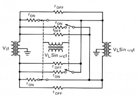
Figure 5: Equivalent circuit for commutation mixer
The effect of \(r_{DS}\) of the MOSFETs may be determined from the analysis of the equivalent circuit shown in Figure 5, assuming that our local oscillator is an idealized square wave. It is not, but if we assume that it is, our analysis is greatly simplified; and for a commutation mixer, a high local oscillator voltage begins to approach the ideal waveform of a square wave.
Figure 5, showing switches rather than MOSFETs, also identifies the ON state resistance, \(r_{DS}\), as well as the OFF state resistance, \(r_{OFF}\). The latter can be disregarded in this analysis as it is generally extremely high (\(\gt 2\times 10^9\Omega\)). On the other hand the ON state resistance, \(r_{DS}\), together with the source and load impedances (i.e. signal and intermediate frequency impedances) directly affects the conversion efficiency.
If we assume that our local oscillator excitation is an idealized square wave, the switching action may be represented by the Fourier series as,
The switching function, \(\epsilon(t)\), shown in the equivalent derivative circuit in Figure 6, is derived from the magnitude of this Fourier series expansion as a power function by squaring the first term, i.e. \((2/\pi)^2\).
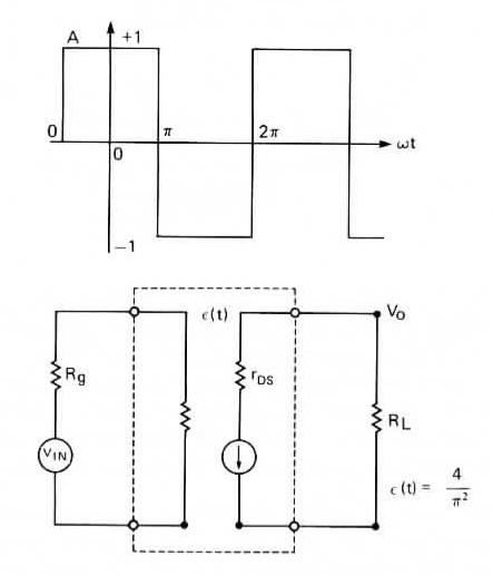
Figure 6: Derivative equivalent circuit
The available power that can be delivered from a generator of RMS open circuit terminal voltage, \(V_{in}\), and internal resistance, \(R_g\), is
or, in terms of Figure 7,
the output power, deliverable to the intermediate frequency port, is
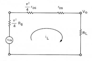
Figure 7: The power loop circuit with all elements equivalent based on the transfer function \(\epsilon(t) = 4 / \pi^2\)
To arrive at \(V_0\), we first need to obtain the loop current, \(i_L\), which from Figure 7 offers
then
Combining these two equations,
Conversion efficiency - in the case for the commutation mixer, a loss - may be calculated from the ratio \(P_{av}\) and \(P_{out}\)
The conversion loss represented by equation (3) is for a broadband double balanced mixer with all ports matched to the characteristic line impedances. The ideal commutating mixer operating resistive source and load impedances will result in having the image and all harmonic frequencies dissipated. For this case, the optimum conversion loss reduces to
or \(-3.92\) dB.
However, a truly optimum mixer also demands that the MOSFETs exhibit an ON state resistance of zero ohms and, of course, an ideal square wave excitation. Neither is possible in a practical sense.
Equation (3) can be examined for various values of source and load impedances as well as \(r_{DS}\) by a graphical representation, as shown in Figure 8 remembering that a nominal 3.92 dB must be added to the values obtained from this graph.
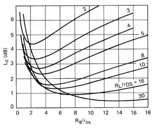
Figure 8: Insertion loss as a function of \(r_{DS}\), \(R_L\), and \(R_g\)
To illustrate how seriously the ON state resistance of the MOSFETs affects performance, we need only to consider the Si8901 with a nominal \(r_{DS}\) (at \(V_{GS}\) = 15V) of 23 ohms. With a 1:1 signal transformer (50 to 25-0-25 \(\Omega\)), \(R_g/r_{DS} = 1.1\). Allowing a 4:1 IF output transformer to a 50-ohm preamplifier, the ration \(R_L/r_{DS}\) approximates 4. From Figure 8 we read a conversion loss, \(L_c\), of approximately 3.7 dB, to which we add 3.92 dB for a total loss of 7.62 dB. Additionally, we must also include the losses incurred by both the signal and IF transformers. The result compares favourably with measured data.
A careful study of Figure 8 reveals what appears to be an anomalous characteristic. If we were to raise \(R_g/r_{DS}\) from 1.1 to 4.3 (by replacing the 1:1 transformer with a 1:4 to effect a signal source impedance of 100-0-100 \(\Omega\)), we would see a dramatic improvement in conversion efficiency. The anomaly is that this suggests that a mismatched signal input port improves performance.
Intermodulation distortion
Unbalanced, single balanced, and double balanced mixers are distinguished by their ability to selectively reject spurious frequency components, as defined in Table 3. The double balanced mixer, by virtue of its symmetry, suppresses twice the number of spurious frequencies as the single balanced mixer suppresses.
Single Balanced |
Double Balanced |
|---|---|
\(f_s\) |
|
\(3f_s\) |
|
\(5f_s\) |
|
\(f1\pm f2\) |
\(f1\pm f2\) |
\(f1\pm 3f2\) |
\(f1\pm 3f2\) |
\(f1\pm 5f2\) |
\(f1\pm 5f2\) |
\(2f1\pm f2\) |
|
\(3f1\pm f2\) |
\(3f1\pm f2\) |
\(3f1\pm 3f2\) |
\(3f1\pm 3f2\) |
\(4f1\pm f2\) |
|
\(5f1\pm f2\) |
\(5f1\pm f2\) |
In the ideal mixer, the input signal is translated to an intermediate frequency without distortion, that is without impairing any of the contained information. Regrettably, the ideal mixer does not occur in practice. Because of certain non-linearities within the switching elements (MOSFETs in this case) as well as imperfect switching resulting in phase modulation, distortion results.
Identifying intermodulation distortion products
The most damaging intermodulation distortion (IMD) products in receiver design are generally those attributed to odd-order and, in particular, those identified as the third order IMD.
Any non-linear device may be represented as a power series
which can be broken into
Term |
Output |
Transfer Characteristic |
|---|---|---|
\(g_me_g\) |
F1, F2 |
Linear |
\(\frac{1}{2!}\frac{\delta gm}{\delta V_G}e_G^2\) |
2F1, 2F2 |
Second-order |
F1 ± F2 |
Square-law |
|
\(\frac{1}{3!}\frac{\delta gm}{\delta V_G}e_G^3\) |
3F1, 3F2 |
|
2F1 ± F2 |
Third order |
|
2F2 ± F1 |
The second order term is the desired intermediate frequency we seek, all other higher orders are undesirable but, unfortunately, are present to a varying degree as illustrated in Figure 9.
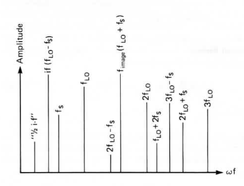
Figure 9: The harmonic and spurious content exiting the IF port of the commutation mixer
There are both fixed level IMD products and level dependent IMD products. The former are produced by the interaction between a fixed level signal, such as the local oscillator and the variable amplitude signal. The resulting frequencies may be identified by
where \(n\) is an integer greater than 1.
Level dependent IMD products result from the interaction of the harmonics of the local oscillator and those of the signal. The resulting frequencies may be identified by
where \(m\) and \(n\) are integers greater than 1.
For a mixer to generate IMD products at the intermediate frequency, we must account for at least a two step process. First, the generation of the harmonics of the signal and local oscillator; and second, the mixing or conversion of these frequencies to the intermediate frequency. Consequently, the mixer may be modelled as a series connection of two non linear impedances, the first to generate the harmonic products and the second to mix or convert to the intemediate frequency. Although many harmonically related products are possible, we will focus principally on the odd order IMD products.
If we allow two interfering signals, \(f_1\) and \(f_2\), to impinge upon the first non-linear element of our mixer model, the result will be \(2f_1 - f_2\) and \(2f_2 - f_1\). These are identified as third order intermodulation products. Other products are also genererated taking the form \(3f_1 - 2f_2\) and \(3f_2 - 2f_1\), called fifth order IMD products. Unlike the even order products, odd order products lie close to the fundamental signals and, as a consequence, are most susceptible to falling within the passband of the intermediate frequency and thus degrading the performance of the mixer.
A qualitative definition of linearity based upon intermodulation distortion performance is called the intercept point. Convergence occurs when
the fundamental output (IF) response is directly proportional to the signal input level.
the second order output response is proportional to the square of the signal input level; and,
the third order output response is proportional to the cube of the signal input level.
The point of convergence is termed the intercept point. The higher the value of the intercept point, the better the dynamic range.
Intermodulation distortion in the commutation mixer
Although the double balanced mixer outperforms the single balanced mixer as we saw in Table 3, a more serious source of intermodulation products results when the local oscillator excitation departs from the idealized square wave. This phenomena is easily recognised by a careful examination of Figure 10, where a sinusoidal local oscillator voltage reacts not only upon a varying transfer characteristic but also on a non linear, voltage dependent capacitance (not shown in Figure 10). Although the effects of this sinusoidal transition are not easily derived, Ward (A Wide Dynamic Range Single Sideband Receiver) and Rafuse (Symmetric MOSFET Mixers of High Dynamic Range) have concluded that lowering \(R_g\) will provide improved intermodulation performance! This conflicts with low conversion loss, as we saw in Figure 8, but agrees with equation (4).
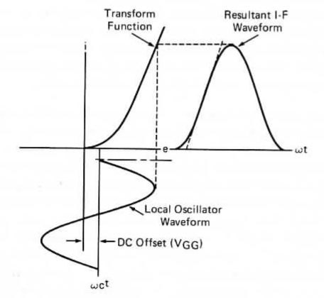
Figure 10: Effect of sinusoidal LO waveform on IF linearity.
Further examination of Figure 10 reveals that the sinusoidal local oscillator excitation results in phase modulation. That is, as the sinusoidal wave goes through a complete cycle, the resulting gate voltage, acting upon the MOSFET's transfer characteristic, produces a resulting non linear waveform. Since all FETs have some offset - a JFET has cut-off voltage, and a MOSFET has threshold voltage - it is important, both for symmetry as well as for balance, to offer some dc offset voltage to the gates. Optimum IMD perfoemance demands that the switches operate at 50% duty cycle; that is, the switches must be fully ON and fully OFF for equal time. Without some form of offset bias, this would be extremely difficult unless we were to implement an idealized square wave drive.
Walker (Sources of Intermodulation in Diode-Ring Mixers) has derived an expression showing the predicted improvement in the relative level of two tone third order intermodulation products as a function of the rise and fall times of the local oscillator waveform.
where, \(V_c\) is the peak-to-peak local oscillator voltage, \(V_s\) is the peak signal voltage, \(t_r\) is the rise and fall time of \(V_c\), \(\omega_{LO}\) is the local oscillator frequency.
Equation (4) offers us several intereting aspects on performance. Since any reduction in the magnitude of \(V_s\) improves IMD, we again discover that by lowering \(R_g\) (which, in turn, decreases the magnitude of \(V_s\)) appears to benfit performance. Second, the higher the local oscillator voltage, the better the IMD performance. Third, if we can provide the idealized square wave drive, we achieve an infinite improvement in IMD performance!