A Wideband, High Linearity IF Amplifier.
Features
Although not commonly considered for IF amplifiers, wideband operational amplifiers can offer considerable performance advantages at the lower IF (or HF) over standard AC coupled MMIC amplifiers.
Flat 20 dB gain up to \(\sim\) 100 MHz, -3 dB at 70 MHz for 27 dB gain.
High linearity and low distortion up to \(\sim\) 50 MHz: OIP3 > 25 dB and HD3 < -70 dBc at 50 MHz
Customizable gain.
Good input and output impedance matching: S11and S22< -22 dB up to 100 MHz.
Excellent reverse isolation: < -70 dB up to 100 MHz.
Single supply design and low quiescent supply current: 22 mA at 10V.
Typical Performance Characteristics
Gain compression and OIP3
Figures 1a and 1b show measurements of output power against input power for the amplifier with gain 27 dB at 10.7 MHz. The -1 dB compression point output power for the supply voltages +5V, +8V and +10V is listed in Table 1.
Variation of OP1dB with increasing signal frequency is an effect caused by the finite slew rate of the opamp.
Figure 1a: Amplifier output power vs. input power for supply voltages 8V and 10V. Measured at 10.7 MHz.
Figure 1b: Variation of -1 dB compression point with signal frequency (\(V_s\) = 10V, amplifier gain = 27 dB).
Supply Voltage, \(V_s\) |
Output power (dBm) |
|---|---|
+5V |
5.6 |
+8V |
14.3 |
+10V |
16.4 |
Figure 3a: Output 2-tone 3rd order intermodulation intercept for \(V_s\) = 10V.
Figure 3b: Output 2-tone 3rd order intermodulation intercept for \(V_s\) = 8V.
Harmonic Distortion
The OPA847 datasheet doesn't specify levels of harmonic distortion for 50 \(\Omega\) impedances. The expected levels of distortion at the power levels for which this amplifier would most likely be used are also not specified in the data sheet. For these reasons some time was spent measuring the distortion products of the prototype amplifiers.
Figure 5a: Harmonic distortion for Vs= 10V.
Figure 5b: Harmonic distortion for Vs= 8V.
Figure 5c: Harmonic distortion for Vs= 5V.
S-Parameters
Figure 6: IF amplifier S-parameter measurements.
Design Notes
Circuit Design
Figure 7: Amplifier schematic design.
The circuit is a non-inverting variant of the single supply design outlined
in the OPA847 datasheet. Power supply conditioning is included in the form
of filtering on the power input (C1, R1, C2) and an optional
voltage regulator (U1, C3, C4, C6). If regulation is done off board
U1 can be replaced with a 0 \(\Omega\) jumper (R26) while retaining the
decoupling provided by C3, C4 and C2.
When U1 is replaced with a 0 \(\Omega\) jumper, the supply voltage can be
set from +5V to +12V (refer to the OPA847 datasheet, p15,
'Single Supply Operation'). The prototype amplifiers were tested using supply
voltages of +5V, +8V and +10V. For a +10V supply voltage and using the output
voltage and current limitations as specified in the graph on p 7 of the OPA847
datasheet, a rough estimate of 14 dB for the -1 dB compression point can be made.
If higher output power is required then increasing supply voltage
to +12V will allow a slight increase in the compression point.
Amplifier gain is set with R6 and R7. For the prototype amplifiers
three gain settings were tested as listed in Table 1. Note that 6 dB of the
gain as calculated from R6 and R7 is lost from the amplifier output
to the load. The resulting overall gain is listed in Table 1.
Gain (dB) |
|
|
|---|---|---|
14 |
39 |
360 |
20 |
39 |
820 |
27 |
39 |
1.8k |
Connector |
Jumper |
|---|---|
Input SMA edge launch ( |
|
Input MMCX RA ( |
|
Output SMA edge launch ( |
|
Output MMCX RA ( |
|
Provision is made for an input network to allow for filtering and/or
attenuation of the input signal (X1 to X5). The design also allows
for either edge launch or right angle SMA connectors for input and output
signals. These are chosen by populating the associated jumpers as shown
in Table 2.
With the chosen resistor values (R4, R5, R6) it's possible to estimate
the total input referred noise voltage, with resistors, as
\(1.4\textrm{nV}/\sqrt{\textrm{Hz}}\) (using equation (11) from the OPA847
datasheet). The noise figure for the amplifier can now be approximated.
Details for this are contained in Calculating Noise Figure in Opamps.
Carrying through this calculation for the prototype design yields a
noise figure of about 11 dB.
The dynamic range for a typical application of the amplifier can now be estimated. The power of the minimum discernable signal will be given by:
where \(G_A\) is the gain of the amplifier, NF is the noise figure and \(B\) is the noise bandwidth. Taking a bandwidth of interest from 10 MHz to 20 MHz together with an amplifier gain of 20 dB and the estimated noise figure of 11 dB produces:
Now using the -1 dB compression point of 14 dB as the maximum usable output power, the amplifier dynamic range will be approximately 87 dB.
PCB layout
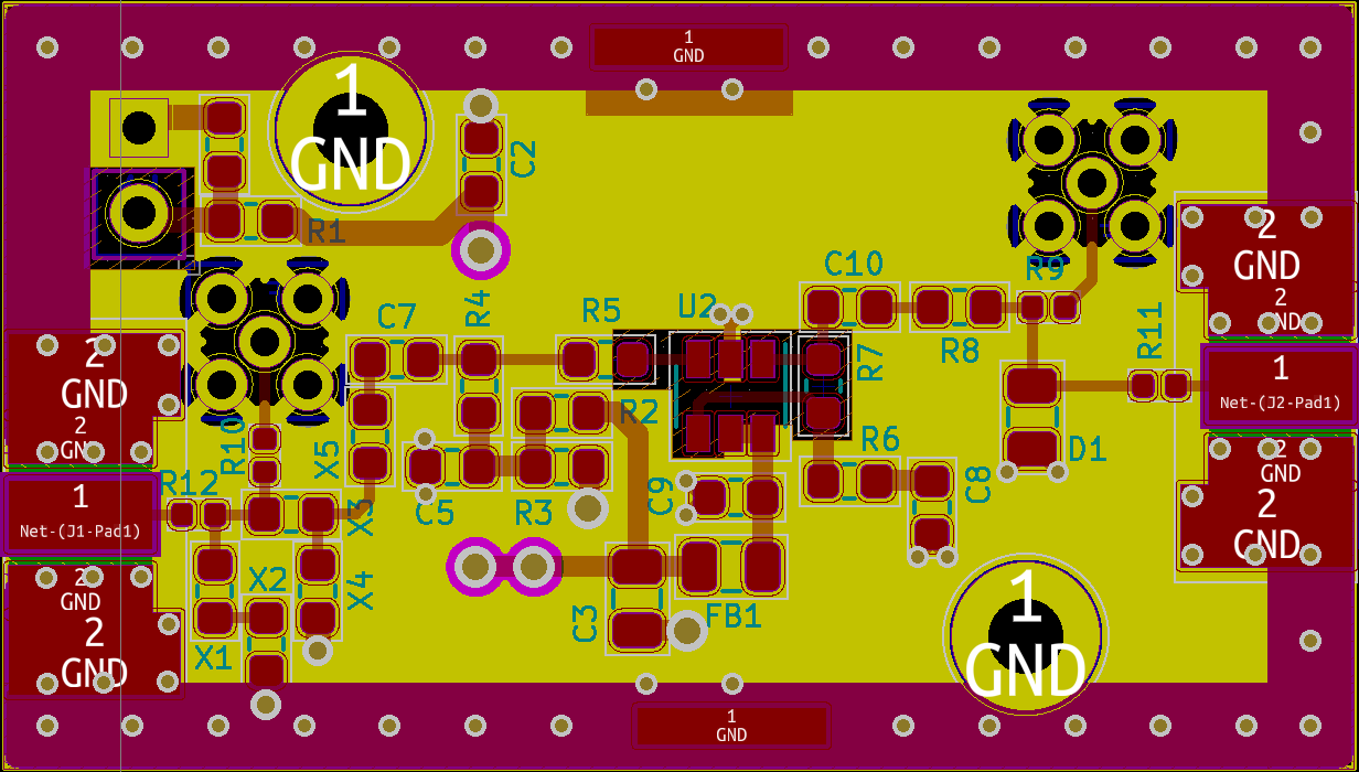
The general layout of the amplifier board is shown in Figure 2a. From the opa847 datasheet (Board Layout section):
To reduce unwanted capacitance, create a window around the signal I/O pins in all of the ground and power planes around these pins. Otherwise, ground and power planes should be unbroken elsewhere on the board.
Figure 2a: IF Amp. module layout.

Figure 2b: IF Amp. PCB layout.