
Using DMA on the Red Pitaya Board
DMA Design
The Xilinx AXI DMA core is used to implement the DMA engine. In the test design the core is configured as follows:
# ...
cell xilinx.com:ip:axi_dma:7.1 axi_dma_0 {
    c_include_sg 0
    c_sg_include_stscntrl_strm 0
    c_include_mm2s 0
    c_sg_length_width 23
} {
    s2mm_introut ps_0/IRQ_F2P
}
# ...
Note that the core is configured with only a write channel and no scatter gather functionality. The buffer length register is set to 23 bits (the maximum) which allows for large data transfers. The other core configuration parameters are left as their default values.
Test Bench
This test consists of a known signal source, in this case a DDS unit, feeding the input of the DMA unit and also the Red Pitaya DAC. This allows a direct comparison between the output of the DAC and the data read via the DMA.

Block design of the DMA test bench
Some things worth noting here:
-
This design makes use of the ADC clock throughout the PL fabric. The
CLK0port is therefore disabled in the processing system block: The DDS clock is the 125 MHz ADC clock.
The final size of the phase increment word is 28 bits.
The DAC clock is derived from the ADC clock via the PLL clock wizard
pll_0and is 125 MHz with DDR clock being 250 MHz.
The input to the S_AXIS_S2MM interface of the DMA unit comes directly
from the broadcaster which in turn takes it's input from the DDS output.
cell xilinx.com:ip:axis_broadcaster:1.1 bcast_0 {
    S_TDATA_NUM_BYTES.VALUE_SRC USER
    M_TDATA_NUM_BYTES.VALUE_SRC USER
    S_TDATA_NUM_BYTES 4
    M_TDATA_NUM_BYTES 4
    M00_TDATA_REMAP {tdata[31:0]}
    M01_TDATA_REMAP {tdata[31:0]}
} {
    S_AXIS dds_0/M_AXIS_DATA
    M01_AXIS axi_dma_0/S_AXIS_S2MM
    aclk pll_0/clk_out1
    aresetn /rst_0/peripheral_aresetn
}
The other output from the broadcaster goes directly to the DAC unit.
The DDS compiler block is explicitly configured to generate sine and cosine outputs. The format of the output stream is therefore:
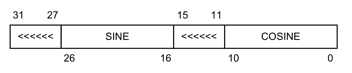
At the DAC, the sine and cosine sub-streams are converted to analog signals on outputs DAC 1 and DAC 2.
Image Build
The image build is straightforward with a small modification required to the generated device tree in order to support the DMA device driver.
The device tree
The device tree produced by the Xilinx tools will need to be modified in
order to work correctly with the DMA kernel driver. The pl.dtsi file
(included in the system.dts file) has to be patched in order to include
character device which acts to control the DMA driver. The following
patch is applied:
13a14,18
>                 axidma_chrdev: axidma_chrdev@0 {
>                         compatible = "xlnx,axidma-chrdev";
>                         dmas = <&axi_dma_0 0>;
>                         dma-names = "rx_channel";
>                 };
The build rule for system.dts is modified to include the required patching:
The output products
By default the build products are copied to the
Source/red-pitaya-notes directory. From there the required files may
be copied to the TFTP server files area (/var/lib/tftp).
If desired, the makefile may also be modified to add commands that copy the required build output products to the TFTP server files area. The relevant parts are:
uImage: $(LINUX_DIR)
        make -C $< mrproper
        make -C $< ARCH=arm xilinx_zynq_defconfig
        make -C $< ARCH=arm CFLAGS=$(LINUX_CFLAGS) \
          -j $(shell nproc 2> /dev/null || echo 1) \
          CROSS_COMPILE=arm-linux-gnueabihf- UIMAGE_LOADADDR=0x8000 uImage modules
        cp $</arch/arm/boot/uImage $@
        cp $</arch/arm/boot/uImage $(TFTPBOOT_DIR)
# ...
devicetree.dtb: uImage tmp/$(NAME).tree/system.dts
        $(LINUX_DIR)/scripts/dtc/dtc -I dts -O dtb -o devicetree.dtb \
          -i tmp/$(NAME).tree tmp/$(NAME).tree/system.dts
        cp devicetree.dtb $(TFTPBOOT_DIR)
# ...
tmp/%.bit: tmp/%.xpr
        mkdir -p $(@D)
        $(VIVADO) -source scripts/bitstream.tcl -tclargs $*
        cp $@ $(TFTPBOOT_DIR)/fpga.bit
This makes the images available for download via TFTP to the target board.
DMA Kernel Driver
The Xilinx AXI DMA kernel driver (and user space library) from here: https://github.com/bperez77/xilinx_axidma was forked and a number of patches applied. These patches were primarily required in order to get the driver working with Linux 6.x kernel versions. The fork is available here: https://gitlab.com/dyadic/xilinx-axidma.
(For reference, the Xilinx 'Soft DMA Driver' documentation is available here: https://xilinx-wiki.atlassian.net/wiki/spaces/A/pages/18842337/Linux+Soft+DMA+Driver)
Device tree bindings documentation are here:
https://github.com/Xilinx/linux-xlnx/blob/master/Documentation/devicetree/bindings/dma/xilinx/xilinx_dma.txt.
In the axidma_chrdev dmas property it's worth noting that previous
versions of the device tree bindings expected (or allowed) the channel id
to be 0 if only one dma channel was defined. Now the channel id must
be '0' for write/tx and '1' for read/rx channel.
Building the driver and user space library
Clone the source repo:
The kernel driver is built using:
timm@rp-dev2:~/Source/xilinx_axidma$ make CROSS_COMPILE=arm-linux-gnueabihf- ARCH=arm KBUILD_DIR=../red-pitaya-notes/tmp/linux-6.1 driver
make -C ../red-pitaya-notes/tmp/linux-6.1 M=/home/timm/Source/xilinx_axidma/driver modules
make[1]: Entering directory '/home/timm/Source/red-pitaya-notes/tmp/linux-6.1'
  CC [M]  /home/timm/Source/xilinx_axidma/driver/axi_dma.o
  CC [M]  /home/timm/Source/xilinx_axidma/driver/axidma_chrdev.o
  CC [M]  /home/timm/Source/xilinx_axidma/driver/axidma_dma.o
  CC [M]  /home/timm/Source/xilinx_axidma/driver/axidma_of.o
  LD [M]  /home/timm/Source/xilinx_axidma/driver/axidma.o
  Building modules, stage 2.
  MODPOST 1 modules
  CC [M]  /home/timm/Source/xilinx_axidma/driver/axidma.mod.o
  LD [M]  /home/timm/Source/xilinx_axidma/driver/axidma.ko
make[1]: Leaving directory '/home/timm/Source/red-pitaya-notes/tmp/linux-6.1'
The user space library is built using:
timm@rp-dev2:~/Source/xilinx_axidma$ make CROSS_COMPILE=arm-linux-gnueabihf- ARCH=arm library
arm-linux-gnueabihf-gcc -Wall -Wextra -Werror -std=gnu99 -g -O0 -fPIC -shared -Wno-missing-field-initializers -I include library/libaxidma.c -o library/libaxidma.so
The axidma_read example utility is now built using:
Testing
The red pitaya board is booted over TFTP using the usual procedure.
Depending on the application being targeted, the contiguous memory
allocation (CMA) may require modification. The default size of the CMA
is set to 16MiB (as defined by the CONFIG_CMA_SIZE_MBYTES kernel
configuration parameter. This may be changed by modifying the kernel
configuration prior to a rebuild. More conveniently, the CMA size may
also be changed by adding the U-boot bootargs specification:
cma=<size>M. This can be done by editing boot-rp.txt file and
re-building the U-boot boot script as described in the Set up Netboot for the Xilinx
2020.1 U-Boot section of the Red Pitaya Development Environment page.
After the target board successfully boots copy the products of the DMA driver build over:
Log in to the board and load the kernel module:
root@redpitaya:~# cd outputs
root@redpitaya:~/outputs# insmod axidma.ko
axidma: axidma_dma.c: axidma_dma_init: 706: DMA: Found 0 transmit channels and 1 receive channels.
axidma: axidma_dma.c: axidma_dma_init: 708: VDMA: Found 0 transmit channels and 0 receive channels.
root@red-pitaya:/home/dyadic/Source/dma_test/kernel/xilinx_axidma/driver# lsmod
Module                  Size  Used by
axidma                 28672  0
...
As shown above by the console messages, the driver module should find only the one DMA receive channel.
Setting the DDS output Frequency
First, the source code for the set_phase utility is copied over to
the target Red Pitaya board and built:
scp -r software/rpboard/dma_test/app/set_phase.c root@redpitaya:~
# Log in to the target board and build the set_phase utility:
gcc set_phase.c -o set_phase
For the dma_test design the DDS clock frequency is 125 MHz and the
phase increment word size is 28 bits, the phase increment which gives an
output frequency of 1 MHz is:
The value produced is then loaded into the DDS phase increment configuration register using:
The measured frequency of the signal on output A of the board is then
seen to be: 999.9865 kHz
The DAC outputs
The two DAC outputs are expected to be offset by a phase of \(90^{\circ}\). This is checked by explicit measurement as illustrated below:
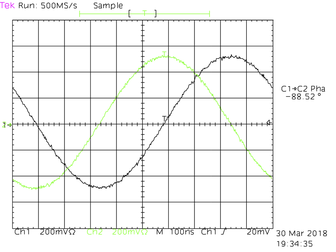
On the Tek784 the measured phase difference is ~90 degrees.
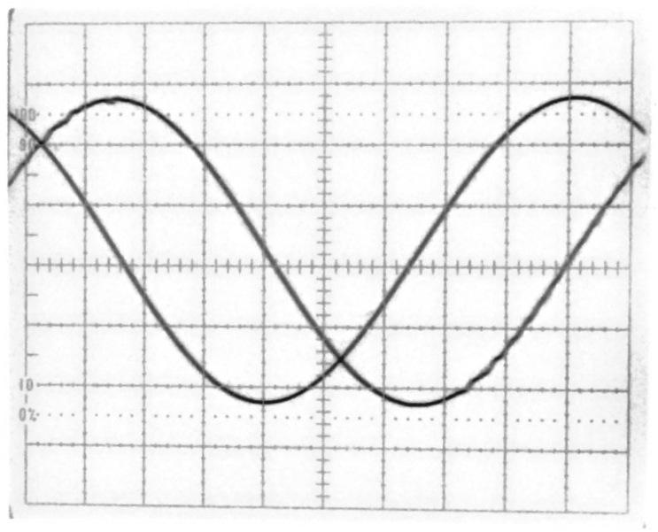
On the Tek485 with timebase 0.1nS the phase difference is measured as 2.5 units.
A DMA read
An experimental DMA read can now be carried out
./axidma_read data.out 8192
AXI DMA File Transfer Info:
Receive Channel: 0
Output File Size: 0.01 Mb

Writing output data to `data.out`.
The output data can be put in a form which is more usable using the following:
Note that the data is being read as a series of signed 16-bit quantities. This matches the output stream format of the DDS.
Dumping a selection of the data produces the following:
a[200:500:2]
array([-1324, -1132,  -931,  -734,  -523,  -323,  -116,    97,   292,
       498,   710,   913,  1108,  1306,  1489,  1686,  1867,  2054,
       2226,  2402,  2557,  2716,  2872,  3012,  3144,  3277,  3393,
       3502,  3608,  3699,  3783,  3856,  3922,  3976,  4020,  4055,
       4079,  4093,  4096,  4089,  4071,  4044,  4007,  3958,  3900,
       3834,  3753,  3668,  3572,  3466,  3354,  3223,  3099,  2960,
       2813,  2659,  2508,  2335,  2167,  1978,  1799,  1611,  1418,
       1228,  1035,   833,   629,   423,   217,    16,  -192,  -398,
       -604,  -802, -1004, -1204, -1395, -1594, -1782, -1961, -2141,
       -2315, -2478, -2640, -2795, -2943, -3083, -3215, -3332, -3449,
       -3559, -3654, -3743, -3820, -3892, -3948, -4000, -4038, -4068,
       -4087, -4096, -4094, -4082, -4059, -4025, -3983, -3931, -3868,
       -3795, -3709, -3620, -3518, -3411, -3296, -3160, -3029, -2885,
       -2739, -2581, -2422, -2247, -2076, -1900, -1714, -1524, -1324,
       -1126,  -931,  -734,  -529,  -323,  -116,    91,   298,   498,
       710,   907,  1108,  1306,  1495,  1686,  1872,  2054,  2226,
       2397,  2567,  2720,  2872,  3007,  3148], dtype=int16)
This dumps some of the data points for one of the DDS signals in the stream. To visualize the data some further processing is required:
import matplotlib.pyplot as plt
b = a / 4096.0
c = b[1::2]         # Separate the signals
d = b[::2]
plt.plot(c, "-b")
plt.plot(d, "-r")
plt.show()
c = b[1:200:2]
d = b[:200:2]
plt.plot(c, "-b")
plt.plot(d, "-r")
plt.show()
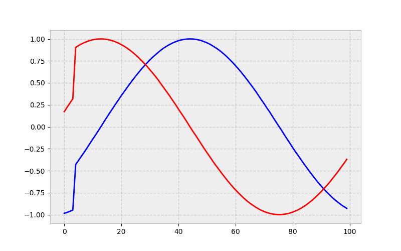
This produces the following plots:
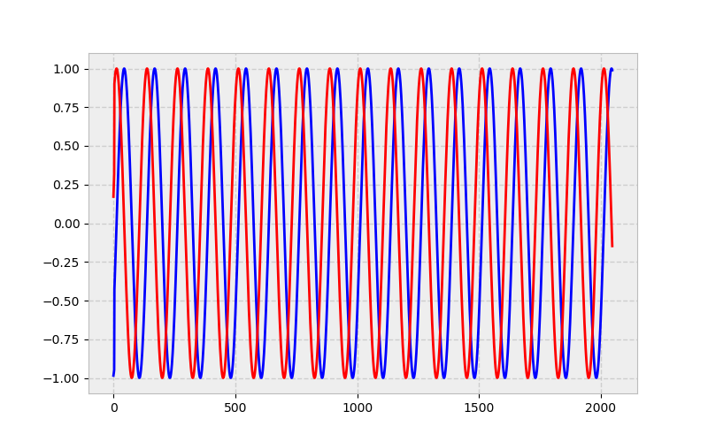
DDS data as read from the DMA unit.
DDS data at the beginning of the DMA read.
Note that latency within the DMA unit will cause the first 5 to 10 data values to be invalid. After that the data is as expected.
axidma Python module
The C foreign function interface (cffi) is used to build Python bindings
for the axidma driver user space code. The CFFI "out-of-line", "API
mode" is used to build the _axidma module. Source code for the module
build is contained in xilinx_axidma/python/axidma_extension_build.py.
Details on using CFFI in this context can be found here:
ffibuilder.set_source(): preparing out-of-line modules.
The _axidma is built on the RP board using the following procedure:
-
After logging into the
dyadic@red-pitayaaccount activate therpboardPython virtual environment: -
Build the module:
This will produce a shared object in the build directory
-
Copy the module into the virtual environment
site_packagesarea:
Testing the module
>>> import os
>>> from os import O_WRONLY, O_CREAT, O_TRUNC
>>> import _axidma
>>> from _axidma import ffi
>>> import numpy as np
>>> axidma_dev = _axidma.lib.axidma_init()
>>> rx_chans = _axidma.lib.axidma_get_dma_rx(axidma_dev)
>>> input_channel = rx_chans.data[0]
>>> output_size = 8192
>>> output_buf = _axidma.lib.axidma_malloc(axidma_dev, output_size)
>>> rc = _axidma.lib.axidma_oneway_transfer(axidma_dev, input_channel, output_buf, output_size, True)
>>> output_fd = os.open('data.bin', O_WRONLY|O_CREAT|O_TRUNC)
>>> os.write(output_fd, ffi.buffer(output_buf, output_size))
8192
>>> os.close(output_fd)
>>> a = np.frombuffer(ffi.buffer(output_buf, output_size), dtype=np.int16)
>>> a[200:500:2]
array([ 3663,  3562,  3462,  3343,  3227,  3087,  2956,  2808,  2654,
        2488,  2320,  2157,  1978,  1799,  1605,  1412,  1216,  1023,
         821,   610,   411,   210,     9,  -204,  -411,  -617,  -821,
       -1017, -1216, -1412, -1605, -1782, -1972, -2151, -2325, -2488,
       -2649, -2799, -2951, -3087, -3219, -3340, -3459, -3562, -3660,
       -3746, -3825, -3896, -3952, -4001, -4040, -4069, -4088, -4096,
       -4093, -4080, -4057, -4024, -3980, -3928, -3864, -3793, -3709,
       -3614, -3512, -3400, -3284, -3160, -3024, -2885, -2725, -2577,
       -2412, -2242, -2071, -1889, -1697, -1506, -1324, -1120,  -925,
        -722,  -517,  -311,  -104,   104,   304,   511,   710,   919,
        1108,  1312,  1506,  1691,  1878,  2060,  2236,  2402,  2562,
        2720,  2872,  3016,  3156,  3281,  3404,  3512,  3611,  3707,
        3788,  3862,  3924,  3979,  4023,  4056,  4081,  4093,  4096,
        4088,  4070,  4042,  4003,  3957,  3896,  3829,  3748,  3666,
        3565,  3459,  3347,  3219,  3091,  2947,  2808,  2649,  2493,
        2325,  2157,  1972,  1788,  1611,  1412,  1222,  1017,   827,
         617,   417,   204,    -3,  -198,  -405], dtype=int16)
>>> _axidma.lib.axidma_free(axidma_dev, output_buf, output_size)
>>> _axidma.lib.axidma_destroy(axidma_dev)
Zero copy buffering
The DMA engine used in these designs makes use of a kernel driver which
implements 'zero copy' buffering. In the test code presented in the
previous section, the output_buffer contains the data as returned by
the DMA hardware. There is no copying of the data from kernel to user
space.
In order to extend this zero copy approach into the user space
processing the following code is used to create a numpy array which
accesses the underlying data in the output_buffer. The numpy dtype
is used to inform numpy of the correct representation of the data in the
buffer. In the case of the testing in the previous section the data is
represented as unsigned bytes:
In later testing, the data representation will be as an array of single precision floating point values:
Note that here we are making explicit the 'little endianess' character of the data as transferred by the DMA engine.
In general, the data buffer being used need only be allocated once and the numpy array view only created once. Updates to the underlying buffer may then be accessed via the numpy array:
>>> output_buf = _axidma.lib.axidma_malloc(axidma_dev, output_size)
>>> rc = _axidma.lib.axidma_oneway_transfer(
...     axidma_dev, input_channel, output_buf, output_size, True)
>>> fa = np.frombuffer(ffi.buffer(output_buf, output_size), dtype='<f')
>>> fa
array([ 0.3083179 ,  0.9512832 ,  0.7284651 , ...,  0.36743593,
       -0.63799417,  0.77004087], dtype=float32)
>>> fa[:20]
array([ 0.3083179 ,  0.9512832 ,  0.7284651 ,  0.68508244,  0.9684    ,
        0.24940169,  0.9687655 , -0.24797785,  0.7294713 , -0.684011  ,
        0.30971587, -0.9508289 , -0.18665934, -0.9824245 , -0.6368573 ,
       -0.77098143, -0.92950547, -0.3688078 , -0.99220634,  0.12460399],
      dtype=float32)
>>> fa[20:]
array([-0.8094486 ,  0.5871904 , -0.42644417, ...,  0.36743593,
       -0.63799417,  0.77004087], dtype=float32)
>>> rc = _axidma.lib.axidma_oneway_transfer(
...     axidma_dev, input_channel, output_buf, output_size, True)
>>> fa[:20]
array([-9.92207050e-01,  1.24598265e-01, -8.09452057e-01,  5.87185740e-01,
       -4.26449418e-01,  9.04511213e-01,  6.20511770e-02,  9.98072743e-01,
        5.35201192e-01,  8.44724417e-01,  8.75949264e-01,  4.82402682e-01,
        9.99999523e-01,  7.40885735e-04,  8.76663089e-01, -4.81104255e-01,
        5.36452055e-01, -8.43930483e-01,  6.35299683e-02, -9.97979760e-01],
      dtype=float32)
>>> fa[20:]
array([-0.4251088 , -0.90514207, -0.8085811 , ..., -0.9824265 ,
       -0.6368487 , -0.7709886 ], dtype=float32)
>>> rc = _axidma.lib.axidma_oneway_transfer(
...     axidma_dev, input_channel, output_buf, output_size, True)
>>> fa[:20]
array([ 0.06353569, -0.9979794 , -0.42510355, -0.90514445, -0.80857766,
       -0.5883889 , -0.9920206 , -0.12607384, -0.93005085,  0.3674302 ,
       -0.63799894,  0.77003694, -0.18811464,  0.98214686,  0.3083067 ,
        0.9512868 ,  0.7284571 ,  0.685091  ,  0.968397  ,  0.24941301],
      dtype=float32)
As can be seen from the above output, successive DMA accesses update the numpy array contents transparently without any requirement to actually copy the data.
The usual rules about copy on modify apply to the resulting numpy arrays. Care should be taken to not deallocate the underlying DMA buffer prematurely.
DMA Stream Details
To gain an understanding of the structure of the DMA data stream a simple DMA 'order' test design is used.
DMA byte order
The block structure of this design is shown in the figure below. The associated TCL source for the block design is listed in DMA order test block design.

Block design of the DMA order test bench
A 32 bit wide AXI stream constant is connected to the S_AXIS_S2MM DMA
interface. The 'constant' value is set using the AXI configuration
register which is set up as a generic UIO device.
Running the test image
Project files are contained in software/rpboard/dma_order_test.
These are copied to the red-pitaya-notes/projects directory on the RP
development host and the kernel, FPGA bitsream and kernel device tree
built using the red-pitaya-notes top level make file:
The RP dev. host TFTP server is then updated with the generated files as described in the Updating kernel image, devicetree and/or FPGA bitstream section of the Red Pitaya Development Environment document. The target RP board is then netboot (see the procedure described in Set up Netboot).
After booting, the following commands should be run in order to make the
DMA and UIO devices available (these must be run as the root user,
generally from the serial console):
cd ~/axidma/outputs
insmod axidma.ko
chgrp dyadic /dev/axidma /dev/uio0
chmod g+rw /dev/axidma /dev/uio0
Two small scripts are now used to exercise the UIO configuration memory device and to read data from the DMA channel. Usage and source code are available below in the 'Sources' section.
In the first example cfg_mem.py is used to write a default integer
value (0xdeadbeef) to the configuration memory. The value is written
to memory using the following code:
The integer is written in little endian order.
dma_read.py is now used to read the DMA channel and print out the
first 100 bytes of the received data. This shows that the ordering of
the bytes is again little endian.
$ cd ~Source/scripts
$ python cfg_mem.py -W
cfg_mem[0:4]: 0xef, 0xbe, 0xad, 0xde
$ python dma_read.py
[0xef 0xbe 0xad 0xde 0xef 0xbe 0xad 0xde 0xef 0xbe 0xad 0xde 0xef 0xbe
 0xad 0xde 0xef 0xbe 0xad 0xde 0xef 0xbe 0xad 0xde 0xef 0xbe 0xad 0xde
 0xef 0xbe 0xad 0xde 0xef 0xbe 0xad 0xde 0xef 0xbe 0xad 0xde 0xef 0xbe
 0xad 0xde 0xef 0xbe 0xad 0xde 0xef 0xbe 0xad 0xde 0xef 0xbe 0xad 0xde
 0xef 0xbe 0xad 0xde 0xef 0xbe 0xad 0xde 0xef 0xbe 0xad 0xde 0xef 0xbe
 0xad 0xde 0xef 0xbe 0xad 0xde 0xef 0xbe 0xad 0xde 0xef 0xbe 0xad 0xde
 0xef 0xbe 0xad 0xde 0xef 0xbe 0xad 0xde 0xef 0xbe 0xad 0xde 0xef 0xbe
 0xad 0xde]
In the next example cfg_mem.py is used to write a float value
(3.14159) to configuration memory. The value is written to memory
using the following code:
By default, the byte values of the float are written to the byte array in little endian order.
dma_read.py is now used to read the DMA channel and print out the
first 100 bytes of the received data. This shows the float value
represented as a series of four bytes: 0xd0 0xf 0x49 0x40, in little
endian order. Rerunning dma_read.py to now print the received data as
float values reveals the original float as stored in configuration
memory.
$ python cfg_mem.py -W -f 3.14159
cfg_mem[0:4]: 0xd0, 0xf, 0x49, 0x40
$ python dma_read.py -B
[0xd0 0xf 0x49 0x40 0xd0 0xf 0x49 0x40 0xd0 0xf 0x49 0x40 0xd0 0xf 0x49
 0x40 0xd0 0xf 0x49 0x40 0xd0 0xf 0x49 0x40 0xd0 0xf 0x49 0x40 0xd0 0xf
 0x49 0x40 0xd0 0xf 0x49 0x40 0xd0 0xf 0x49 0x40 0xd0 0xf 0x49 0x40 0xd0
 0xf 0x49 0x40 0xd0 0xf 0x49 0x40 0xd0 0xf 0x49 0x40 0xd0 0xf 0x49 0x40
 0xd0 0xf 0x49 0x40 0xd0 0xf 0x49 0x40 0xd0 0xf 0x49 0x40 0xd0 0xf 0x49
 0x40 0xd0 0xf 0x49 0x40 0xd0 0xf 0x49 0x40 0xd0 0xf 0x49 0x40 0xd0 0xf
 0x49 0x40 0xd0 0xf 0x49 0x40 0xd0 0xf 0x49 0x40]
$ python dma_read.py -F
[3.14159 3.14159 3.14159 3.14159 3.14159 3.14159 3.14159 3.14159 3.14159
 3.14159 3.14159 3.14159 3.14159 3.14159 3.14159 3.14159 3.14159 3.14159
 3.14159 3.14159 3.14159 3.14159 3.14159 3.14159 3.14159 3.14159 3.14159
 3.14159 3.14159 3.14159 3.14159 3.14159 3.14159 3.14159 3.14159 3.14159
 3.14159 3.14159 3.14159 3.14159 3.14159 3.14159 3.14159 3.14159 3.14159
 3.14159 3.14159 3.14159 3.14159 3.14159 3.14159 3.14159 3.14159 3.14159
 3.14159 3.14159 3.14159 3.14159 3.14159 3.14159 3.14159 3.14159 3.14159
 3.14159 3.14159 3.14159 3.14159 3.14159 3.14159 3.14159 3.14159 3.14159
 3.14159 3.14159 3.14159 3.14159 3.14159 3.14159 3.14159 3.14159 3.14159
 3.14159 3.14159 3.14159 3.14159 3.14159 3.14159 3.14159 3.14159 3.14159
 3.14159 3.14159 3.14159 3.14159 3.14159 3.14159 3.14159 3.14159 3.14159
 3.14159]
DDS output stream
The block structure of this design is shown in the figure below. The associated TCL source for the block design is listed in DMA DDS output block design.

Block design of the DMA DDS output test bench
The DDS is configured for an output width of 24 bits, a phase width of 30 bits, and a system clock of 125 MHz. The DDS outputs sine and cosine with a negative sine polarity. The output stream structure is:
# Definition:
struct TDATA(1) {
    fix cosine { bitwidth=24, fractwidth=23}
    fix sine { bitoffset=24, bitwidth=24, fractwidth=23}
} {stride=48, name=chan}

# Layout:
Transaction  Field
0            CHAN_0_SINE(47:24)  fix24_23
             CHAN_0_COSINE(23:0) fix24_23
The phase increment for the DDS is supplied by an AXI stream constant which is configured via the lowest 32 bits of the AXI configuration register. The configuration register is configured as a generic UIO device.
The output from a DDS unit is connected to the S_AXIS_S2MM DMA
interface via an AXI stream subset converter. The subset converter is
used to convert the 6-byte stream output format from the DDS to an 8-byte
stream. The conversion is done according to the following TDATA remap
string:
Running the test image
Project files are contained in software/rpboard/adc_dma_test. These
are copied to the red-pitaya-notes/projects directory on the RP
development host. The file adc_dma_test/block_design_dds.tcl should
then be copied over adc_dma_test/block_design.tcl. The kernel, FPGA
bitsream and kernel device tree are then built using the red-pitaya-notes top
level make file:
The RP dev. host TFTP server is then updated with the generated files as described in the Updating kernel image, devicetree and/or FPGA bitstream section of the Red Pitaya Development Environment document. The target RP board is then netboot (see the procedure described in Set up Netboot).
After booting, the following commands should be run in order to make the
DMA and UIO devices available (these must be run as the root user,
generally from the serial console):
cd ~/axidma/outputs
insmod axidma.ko
chgrp dyadic /dev/axidma /dev/uio0
chmod g+rw /dev/axidma /dev/uio0
The DDS must now be configured with a phase increment word. Using the DDS configuration parameters (set out above), the phase increment word is calculated from:
So, for an output frequency of 1 MHz the phase increment word will be
0x83126e.
The phase increment word is written to the bottom 4 bytes of the configuration register using:
A sample of the DDS output stream is now read as follows:
$ pyenv activate rpboard
$ python
>>> import _axidma
>>> from _axidma import ffi
>>> import numpy as np
>>> axidma_dev = _axidma.lib.axidma_init()
>>> rx_chans = _axidma.lib.axidma_get_dma_rx(axidma_dev)
>>> input_channel = rx_chans.data[0]
>>> output_size = 8192
>>> output_buf = _axidma.lib.axidma_malloc(axidma_dev, output_size)
>>> rc = _axidma.lib.axidma_oneway_transfer(axidma_dev, input_channel, output_buf, output_size, True)
>>> a = np.frombuffer(ffi.buffer(output_buf, output_size), dtype=np.uint8)
>>> a[0:400]
array([176,  30,  23,   0,   8, 229, 125,   0, 207,  50,  22,   0, 117,
        15, 126,   0, 160,  70,  21,   0,  40,  56, 126,   0,  39,  90,
        20,   0,  34,  95, 126,   0, 102, 109,  19,   0,  95, 132, 126,
         0,  97, 128,  18,   0, 225, 167, 126,   0,  27, 147,  17,   0,
       167, 201, 126,   0, 153, 165,  16,   0, 177, 233, 126,   0, 219,
       183,  15,   0, 254,   7, 127,   0, 230, 201,  14,   0, 142,  36,
       127,   0, 189, 219,  13,   0,  95,  63, 127,   0, 100, 237,  12,
         0, 114,  88, 127,   0, 222, 254,  11,   0, 200, 111, 127,   0,
        46,  16,  11,   0,  94, 133, 127,   0,  86,  33,  10,   0,  53,
       153, 127,   0,  91,  50,   9,   0,  77, 171, 127,   0,  64,  67,
         8,   0, 166, 187, 127,   0,   8,  84,   7,   0,  63, 202, 127,
         0, 182, 100,   6,   0,  23, 215, 127,   0,  78, 117,   5,   0,
        48, 226, 127,   0, 211, 133,   4,   0, 136, 235, 127,   0,  72,
       150,   3,   0,  31, 243, 127,   0, 176, 166,   2,   0, 246, 248,
       127,   0,  15, 183,   1,   0,  13, 253, 127,   0, 104, 199,   0,
         0,  98, 255, 127,   0, 190, 215, 255,   0, 248, 255, 127,   0,
        21, 232, 254,   0, 204, 254, 127,   0, 111, 248, 253,   0, 224,
       251, 127,   0, 210,   8, 253,   0,  50, 247, 127,   0,  62,  25,
       252,   0, 196, 240, 127,   0, 184,  41, 251,   0, 150, 232, 127,
         0,  66,  58, 250,   0, 167, 222, 127,   0, 101, 207, 243,   0,
        16, 107, 127,   0, 106, 108, 237,   0,  17, 165, 126,   0, 114,
        21, 231,   0,  46, 141, 125,   0, 151, 206, 224,   0,  25,  36,
       124,   0, 232, 155, 218,   0, 189, 106, 122,   0, 104, 129, 212,
         0,  54,  98, 120,   0,   7, 131, 206,   0, 214,  11, 118,   0,
       167, 164, 200,   0,  31, 105, 115,   0,  21, 234, 194,   0, 199,
       123, 112,   0,   2,  87, 189,   0, 177,  69, 109,   0,  11, 239,
       183,   0, 241, 200, 105,   0, 174, 181, 178,   0, 199,   7, 102,
         0,  77, 174, 173,   0, 163,   4,  98,   0,  39, 220, 168,   0,
        29, 194,  93,   0,  92,  66, 164,   0, 244,  66,  89,   0, 229,
       227, 159,   0,  19, 138,  84,   0, 148, 195, 155,   0, 133, 154,
       79,   0,  22, 228, 151,   0, 126, 119,  74,   0], dtype=uint8)
>>> _axidma.lib.axidma_free(axidma_dev, output_buf, output_size)
>>> _axidma.lib.axidma_destroy(axidma_dev)
The output shows the two DDS streams represented as four bytes for each stream with the sine and cosine values interleaved. As expected, the DDS values are 24 bits with the upper byte of the 4 byte values being set to zero. The values may be converted to signed integers using the following:
>>> ampl = [((a[i+2] if a[i+2] < 128 else (a[i+2]-255)) * 256 + a[i+1]) * 256 + a[i] for i in range(0, 8000, 8)]
>>> ', '.join(ampl)
It is more convenient to view the data as float values. The maximum
amplitude of the DDS output is 1<<23 so the normalized DDS values are
calculated from:
>>> ampl = ['{:.5f}'.format((((a[i+2] if a[i+2] < 128 else (a[i+2]-255)) * 256 + a[i+1]) * 256 + a[i])/max_ampl) for i in range(0, 3200, 8)]
>>> ', '.join(ampl)
'-0.98192, -0.98520, -0.98785, -0.98988, -0.99127, ...
-0.97543, -0.96503, -0.95217'
Since the DDS output frequency was set to 1 MHz we would expect one cycle to be represented by 125 samples:
>>> ', '.join(ampl[50:176])
'0.01997, 0.07018, 0.12021, 0.16994, 0.21924, 0.26798, 0.31605, 0.36332, 0.40967, 0.45499, 0.49916, 0.54206, 0.58360, 0.62367, 0.66215, 0.69897, 0.73402, 0.76721, 0.79847, 0.82771, 0.85486, 0.87985, 0.90262, 0.92310, 0.94126, 0.95704, 0.97040, 0.98131, 0.98974, 0.99567, 0.99908, 0.99997, 0.99834, 0.99418, 0.98751, 0.97835, 0.96671, 0.95264, 0.93616, 0.91731, 0.89614, 0.87271, 0.84708, 0.81931, 0.78947, 0.75763, 0.72388, 0.68830, 0.65098, 0.61202, 0.57151, 0.52956, 0.48627, 0.44175, 0.39612, 0.34948, 0.30197, 0.25369, 0.20476, 0.15533, 0.10550, 0.05540, 0.00516, -0.03728, -0.08741, -0.13731, -0.18684, -0.23588, -0.28430, -0.33198, -0.37881, -0.42466, -0.46941, -0.51296, -0.55520, -0.59601, -0.63530, -0.67296, -0.70891, -0.74304, -0.77528, -0.80553, -0.83374, -0.85982, -0.88370, -0.90534, -0.92466, -0.94164, -0.95621, -0.96835, -0.97802, -0.98520, -0.98988, -0.99203, -0.99166, -0.98876, -0.98335, -0.97543, -0.96503, -0.95217, -0.93688, -0.91921, -0.89920, -0.87690, -0.85236, -0.82565, -0.79683, -0.76598, -0.73318, -0.69850, -0.66204, -0.62389, -0.58414, -0.54290, -0.50026, -0.45634, -0.41125, -0.36511, -0.31801, -0.27010, -0.22148, -0.17229, -0.12264, -0.07266, -0.02248, 0.01997'
DDS floating point output
The design outlined in the previous section is now modified and two
floating point units are inserted. These units are used to convert the
24-bit fixed point format output from the DDS into two streams of single
precision (32-bit) floating point values. These two streams of floating
point values are the combined into a single 8 byte formatted stream which
then forms the input to the S_AXIS_S2MM DMA interface.
The block structure of this design is shown in the figure below. The associated TCL source for the block design is listed in DMA floating point output.
The output data from the above design can be treated as a stream of single precision complex values - each value occupying 8 consecutive bytes in the stream.
>>> fa[:20:2]
array([ 0.9683956 ,  0.9687698 ,  0.72948325,  0.30973244, -0.18664205,
       -0.6368439 , -0.92949903, -0.9922085 , -0.80945885, -0.42646003],
      dtype=float32)
>>> fa[1:21:2]
array([ 0.24941862, -0.24796093, -0.6839982 , -0.95082355, -0.9824277 ,
       -0.7709925 , -0.368824  ,  0.12458658,  0.5871762 ,  0.9045062 ],
      dtype=float32)
>>> fc = np.frombuffer(ffi.buffer(output_buf, output_size), dtype='<F')
>>> fc[:10]
array([ 0.9683956 +0.24941862j,  0.9687698 -0.24796093j,
        0.72948325-0.6839982j ,  0.30973244-0.95082355j,
       -0.18664205-0.9824277j , -0.6368439 -0.7709925j ,
       -0.92949903-0.368824j  , -0.9922085 +0.12458658j,
       -0.80945885+0.5871762j , -0.42646003+0.9045062j ], dtype=complex64)
When converting to complex values as in the above example, numpy will take the first float value to be the real component and the next float to be the imaginary component. The stream in the FPGA block design must be configured with this in mind.
Direct ADC output
When using Pavel Demin's axis_red_pitaya_adc designs the lower 16 bits
are associated with the Red Pitaya ADC 'IN 1' input and the uppper 16 bits
with the ADC 'IN 2' input.
Direct output from the ADC via DMA. Firstly, a 1 MHz signal with an input level of approximately -10 dBm (roughly 170mV into the high impedance Red Pitaya ADC input):
>>> import os
>>> from os import O_WRONLY, O_CREAT, O_TRUNC
>>> import _axidma
>>> from _axidma import ffi
>>> import numpy as np
>>> axidma_dev = _axidma.lib.axidma_init()
>>> rx_chans = _axidma.lib.axidma_get_dma_rx(axidma_dev)
>>> input_channel = rx_chans.data[0]
>>> output_size = 8192
>>> output_buf = _axidma.lib.axidma_malloc(axidma_dev, output_size)
>>> rc = _axidma.lib.axidma_oneway_transfer(axidma_dev, input_channel, output_buf, output_size, True)
>>> ch_array = ffi.cast("char *", output_buf)
>>> byte_array = b''.join(ch_array[i] for i in range(output_size))
>>> a = np.frombuffer(byte_array, dtype=np.int16)
>>> a[200:300]
array([  219,   161,   108,    56,   -11,   -60,  -105,  -174,  -233,
         -287,  -347,  -399,  -454,  -509,  -569,  -608,  -672,  -724,
         -770,  -826,  -865,  -916,  -959,  -996, -1031, -1075, -1108,
         -1149, -1184, -1209, -1229, -1259, -1274, -1303, -1310, -1320,
         -1334, -1341, -1343, -1346, -1351, -1342, -1329, -1319, -1315,
         -1293, -1276, -1256, -1230, -1202, -1171, -1137, -1095, -1069,
         -1016,  -987,  -930,  -898,  -851,  -814,  -755,  -689,  -645,
         -605,  -537,  -488,  -424,  -374,  -311,  -253,  -193,  -129,
         -73,   -18,    36,    97,   149,   208,   260,   311,   358,
         414,   453,   513,   544,   594,   624,   678,   717,   745,
         767,   789,   834,   850,   872,   890,   898,   920,   923,
         925], dtype=int16)
Now a 10 MHz signal with an input level of approximately -10 dBm (roughly 170mV into the high impedance Red Pitaya ADC input):
>>> rc = _axidma.lib.axidma_oneway_transfer(axidma_dev, input_channel, output_buf, output_size, True)
>>> ch_array = ffi.cast("char *", output_buf)
>>> byte_array = b''.join(ch_array[i] for i in range(output_size))
>>> a = np.frombuffer(byte_array, dtype=np.int16)
>>> a[200:300]
array([  248,  -313,  -838, -1190, -1311, -1151,  -767,  -246,   309,
         731,   925,   826,   483,   -26,  -585, -1035, -1290, -1263,
         -990,  -524,    40,   536,   856,   904,   672,   241,  -304,
         -825, -1188, -1306, -1147,  -764,  -236,   308,   720,   923,
         826,   482,   -40,  -579, -1040, -1289, -1271,  -982,  -515,
         40,   531,   849,   907,   690,   239,  -320,  -836, -1203,
         -1305, -1152,  -767,  -235,   311,   728,   914,   827,   490,
         -34,  -578, -1035, -1286, -1263,  -986,  -519,    41,   541,
         862,   919,   672,   243,  -314,  -827, -1199, -1302, -1155,
         -771,  -238,   308,   726,   915,   826,   479,   -34,  -589,
         -1047, -1285, -1260,  -983,  -515,    34,   542,   849,   907,
         685], dtype=int16)
Sources
DMA test block design
The block designn for the DMA_Test4 test bench (with FCLK0 replaced with the ADC clock).
# PLL

# Create clk_wiz
cell xilinx.com:ip:clk_wiz pll_0 {
    PRIMITIVE PLL
    PRIM_IN_FREQ.VALUE_SRC USER
    PRIM_IN_FREQ 125.0
    PRIM_SOURCE Differential_clock_capable_pin
    CLKOUT1_USED true
    CLKOUT1_REQUESTED_OUT_FREQ 125.0
    CLKOUT2_USED true
    CLKOUT2_REQUESTED_OUT_FREQ 250.0
    CLKOUT2_REQUESTED_PHASE -112.5
    CLKOUT3_USED true
    CLKOUT3_REQUESTED_OUT_FREQ 250.0
    CLKOUT3_REQUESTED_PHASE -67.5
    USE_RESET false
} {
    clk_in1_p adc_clk_p_i
    clk_in1_n adc_clk_n_i
}

cell xilinx.com:ip:processing_system7 ps_0 {
    PCW_IMPORT_BOARD_PRESET cfg/red_pitaya.xml
    PCW_EN_CLK0_PORT 0
    PCW_USE_S_AXI_HP0 1
    PCW_USE_FABRIC_INTERRUPT 1
    PCW_IRQ_F2P_INTR 1
} {
    M_AXI_GP0_ACLK pll_0/clk_out1
    S_AXI_HP0_ACLK pll_0/clk_out1
}

# Create all required interconnections
apply_bd_automation -rule xilinx.com:bd_rule:processing_system7 -config {
    make_external {FIXED_IO, DDR}
    Master Disable
    Slave Disable
} [get_bd_cells ps_0]

cell xilinx.com:ip:xlconstant:1.1 const_1

# Create proc_sys_reset
cell xilinx.com:ip:proc_sys_reset rst_0 {} {
    ext_reset_in const_1/dout
}

cell xilinx.com:ip:axi_dma axi_dma_0 {
    c_include_sg 0
    c_sg_include_stscntrl_strm 0
    c_include_mm2s 0
    c_sg_length_width 23
} {
    s2mm_introut ps_0/IRQ_F2P
}

cell pavel-demin:user:axi_cfg_register cfg_0 {
    CFG_DATA_WIDTH 32
    AXI_ADDR_WIDTH 16
    AXI_DATA_WIDTH 32
}

# Create axis_constant
cell pavel-demin:user:axis_constant const_0 {
    AXIS_TDATA_WIDTH 32
} {
    cfg_data cfg_0/cfg_data
    aclk pll_0/clk_out1
}

apply_bd_automation -rule xilinx.com:bd_rule:axi4 -config {
    Master "/ps_0/M_AXI_GP0"
    Clk "Auto"
}  [get_bd_intf_pins cfg_0/S_AXI]

apply_bd_automation -rule xilinx.com:bd_rule:axi4 -config {
    Master "/ps_0/M_AXI_GP0"
    Clk "Auto"
}  [get_bd_intf_pins axi_dma_0/S_AXI_LITE]

apply_bd_automation -rule xilinx.com:bd_rule:axi4 -config {
    Master "/axi_dma_0/M_AXI_S2MM"
    Clk "Auto"
}  [get_bd_intf_pins ps_0/S_AXI_HP0]

# Create dds_compiler
cell xilinx.com:ip:dds_compiler dds_0 {
    PHASE_INCREMENT Streaming
    DDS_CLOCK_RATE 125
    OUTPUT_SELECTION Sine_and_Cosine
    SPURIOUS_FREE_DYNAMIC_RANGE 84
    FREQUENCY_RESOLUTION 0.5
    AMPLITUDE_MODE Unit_Circle
    HAS_PHASE_OUT false
    OUTPUT_FREQUENCY1 0
} {
    S_AXIS_PHASE const_0/M_AXIS
    aclk pll_0/clk_out1
}

# Create axis_broadcaster
cell xilinx.com:ip:axis_broadcaster bcast_0 {
    S_TDATA_NUM_BYTES.VALUE_SRC USER
    M_TDATA_NUM_BYTES.VALUE_SRC USER
    S_TDATA_NUM_BYTES 4
    M_TDATA_NUM_BYTES 4
    M00_TDATA_REMAP {tdata[31:0]}
    M01_TDATA_REMAP {tdata[31:0]}
} {
    S_AXIS dds_0/M_AXIS_DATA
    M01_AXIS axi_dma_0/S_AXIS_S2MM
    aclk pll_0/clk_out1
    aresetn /rst_0/peripheral_aresetn
}

# Create axis_red_pitaya_dac
cell pavel-demin:user:axis_red_pitaya_dac dac_0 {} {
    aclk pll_0/clk_out1
    ddr_clk pll_0/clk_out2
    wrt_clk pll_0/clk_out3
    locked pll_0/locked
    S_AXIS bcast_0/M00_AXIS
    dac_clk dac_clk_o
    dac_rst dac_rst_o
    dac_sel dac_sel_o
    dac_wrt dac_wrt_o
    dac_dat dac_dat_o
}
Setting DDS phase increment
The DDS phase increment is set via the configuration register using the set_phase.c utility.
/*
  command to compile:
  gcc set_phase.c -o set_phase
*/

#include <stdio.h>
#include <errno.h>
#include <stdint.h>
#include <stdlib.h>
#include <string.h>
#include <signal.h>
#include <unistd.h>
#include <sys/mman.h>
#include <fcntl.h>

int interrupted = 0;

void signal_handler(int sig)
{
    interrupted = 1;
}

int main(int argc, char *argv[])
{
    int    mmapfd;
    void  *cfg;
    char  *end, *name = "/dev/mem";
    long   number;
    size_t size;

    if ( (mmapfd = open(name, O_RDWR)) < 0 )
    {
        perror("open");
        return 1;
    }

    cfg = mmap(NULL, sysconf(_SC_PAGESIZE), PROT_READ|PROT_WRITE, MAP_SHARED,
               mmapfd, 0x43C00000);

    errno = 0;
    number = (argc == 2) ? strtol(argv[1], &end, 10) : -1;
    if (errno != 0 || end == argv[1])
    {
        printf("Usage: set_phase phase-incr\n");
        printf("phase-incr - phase increment for DDS\n");
        return EXIT_FAILURE;
    }

    printf(" number=%d\n", number);
    *((uint32_t *)(cfg+0)) = (uint32_t)number;

    signal(SIGINT, signal_handler);

    munmap(cfg, sysconf(_SC_PAGESIZE));

    return EXIT_SUCCESS;
}
DMA read
Synchronous
The following code performs a synchronous DMA read and writes the resulting data to a specified file.
int main(int argc, char **argv)
{
    char *output_path;
    axidma_dev_t axidma_dev;
    struct dma_transfer trans;
    const array_t *rx_chans;

    // Parse the input arguments
    memset(&trans, 0, sizeof(trans));
    if (parse_args(argc, argv, &output_path,
                   &trans.input_channel, &trans.output_size) < 0)
    // ...

    trans.output_fd = open(output_path, O_WRONLY|O_CREAT|O_TRUNC,
                     S_IWUSR|S_IRUSR|S_IRGRP|S_IWGRP|S_IROTH);
    // ...

    // Initialize the AXIDMA device
    axidma_dev = axidma_init();
    // ...

    // Get the rx channel if not already specified
    rx_chans = axidma_get_dma_rx(axidma_dev);
    // ...

    // Read data over the AXI DMA (and write it to the specified output file)
    rc = read_data(axidma_dev, &trans, output_path);
    rc = (rc < 0) ? -rc : 0;

    axidma_destroy(axidma_dev);
    assert(close(trans.output_fd) == 0);
    return rc;
}
The relevant code in the read_data function is:
// Allocate a DMA buffer which is shared between processor and
// FPGA fabric
trans->output_buf = axidma_malloc(dev, trans->output_size);
// ...

// Peform a blocking DMA read
rc = axidma_oneway_transfer(dev, trans->input_channel,
                            trans->output_buf, trans->output_size, true);
// ...

// Write the data to the output file
printf("Writing output data to `%s`.\n", output_path);
rc = robust_write(trans->output_fd, trans->output_buf, trans->output_size);

axidma_free(dev, trans->output_buf, trans->output_size);
It's important to note that axidma_malloc provides a buffer which
allows the DMA data to be passed to the user space library without
copying.
Asynchronous
The following code performs the same task as the synchronous example but in this case the read request is non-blocking and the PS sends an interrupt on completion of the read. This in turn triggers a callback function.
DMA order test block design
# PLL
cell xilinx.com:ip:clk_wiz pll_0 {
    PRIMITIVE PLL
    PRIM_IN_FREQ.VALUE_SRC USER
    PRIM_IN_FREQ 125.0
    PRIM_SOURCE Differential_clock_capable_pin
    CLKOUT1_USED true
    CLKOUT1_REQUESTED_OUT_FREQ 125.0
    CLKOUT2_USED true
    CLKOUT2_REQUESTED_OUT_FREQ 250.0
    CLKOUT2_REQUESTED_PHASE -112.5
    CLKOUT3_USED true
    CLKOUT3_REQUESTED_OUT_FREQ 250.0
    CLKOUT3_REQUESTED_PHASE -67.5
    USE_RESET false
} {
    clk_in1_p adc_clk_p_i
    clk_in1_n adc_clk_n_i
}

cell xilinx.com:ip:processing_system7 ps_0 {
    PCW_IMPORT_BOARD_PRESET cfg/red_pitaya.xml
    PCW_EN_CLK0_PORT 0
    PCW_USE_S_AXI_HP0 1
    PCW_USE_FABRIC_INTERRUPT 1
    PCW_IRQ_F2P_INTR 1
} {
    M_AXI_GP0_ACLK pll_0/clk_out1
    S_AXI_HP0_ACLK pll_0/clk_out1
}

# Create all required interconnections
apply_bd_automation -rule xilinx.com:bd_rule:processing_system7 -config {
    make_external {FIXED_IO, DDR}
    Master Disable
    Slave Disable
} [get_bd_cells ps_0]

cell xilinx.com:ip:xlconstant:1.1 const_1

# Create proc_sys_reset
cell xilinx.com:ip:proc_sys_reset rst_0 {} {
    ext_reset_in const_1/dout
}

cell xilinx.com:ip:axi_dma axi_dma_0 {
    c_include_sg 0
    c_sg_include_stscntrl_strm 0
    c_include_mm2s 0
    c_sg_length_width 23
} {
    s2mm_introut ps_0/IRQ_F2P
}

cell pavel-demin:user:axi_cfg_register cfg_0 {
    CFG_DATA_WIDTH 32
    AXI_ADDR_WIDTH 16
    AXI_DATA_WIDTH 32
}

# Create axis_constant
cell pavel-demin:user:axis_constant const_0 {
    AXIS_TDATA_WIDTH 32
    M_HAS_TLAST 1
} {
    cfg_data cfg_0/cfg_data
    M_AXIS axi_dma_0/S_AXIS_S2MM
    aclk pll_0/clk_out1
}

apply_bd_automation -rule xilinx.com:bd_rule:axi4 -config {
    Master "/ps_0/M_AXI_GP0"
    Clk "Auto"
}  [get_bd_intf_pins cfg_0/S_AXI]

apply_bd_automation -rule xilinx.com:bd_rule:axi4 -config {
    Master "/ps_0/M_AXI_GP0"
    Clk "Auto"
}  [get_bd_intf_pins axi_dma_0/S_AXI_LITE]

apply_bd_automation -rule xilinx.com:bd_rule:axi4 -config {
    Master "/axi_dma_0/M_AXI_S2MM"
    Clk "Auto"
}  [get_bd_intf_pins ps_0/S_AXI_HP0]
DMA DDS output block design
# Create clk_wiz
cell xilinx.com:ip:clk_wiz pll_0 {
    PRIMITIVE PLL
    PRIM_IN_FREQ.VALUE_SRC USER
    PRIM_IN_FREQ 125.0
    PRIM_SOURCE Differential_clock_capable_pin
    CLKOUT1_USED true
    CLKOUT1_REQUESTED_OUT_FREQ 125.0
    CLKOUT2_USED true
    CLKOUT2_REQUESTED_OUT_FREQ 250.0
    CLKOUT2_REQUESTED_PHASE -112.5
    CLKOUT3_USED true
    CLKOUT3_REQUESTED_OUT_FREQ 250.0
    CLKOUT3_REQUESTED_PHASE -67.5
    USE_RESET false
} {
    clk_in1_p adc_clk_p_i
    clk_in1_n adc_clk_n_i
}

# Create processing_system7
cell xilinx.com:ip:processing_system7 ps_0 {
    PCW_IMPORT_BOARD_PRESET cfg/red_pitaya.xml
    PCW_USE_S_AXI_HP0 1
    PCW_USE_FABRIC_INTERRUPT 1
    PCW_IRQ_F2P_INTR 1
} {
    M_AXI_GP0_ACLK pll_0/clk_out1
    S_AXI_HP0_ACLK pll_0/clk_out1
}

# Create all required interconnections
apply_bd_automation -rule xilinx.com:bd_rule:processing_system7 -config {
    make_external {FIXED_IO, DDR}
    Master Disable
    Slave Disable
} [get_bd_cells ps_0]

# Create xlconstant
cell xilinx.com:ip:xlconstant const_0

# Create proc_sys_reset
cell xilinx.com:ip:proc_sys_reset rst_0 {} {
    ext_reset_in const_0/dout
}

cell xilinx.com:ip:axi_dma axi_dma_0 {
    c_include_sg 0
    c_sg_include_stscntrl_strm 0
    c_include_mm2s 0
    c_sg_length_width 23
} {
    s2mm_introut ps_0/IRQ_F2P
}

# ADC

# Create axis_red_pitaya_adc
cell pavel-demin:user:axis_red_pitaya_adc adc_0 {
    ADC_DATA_WIDTH 14
} {
    aclk pll_0/clk_out1
    adc_dat_a adc_dat_a_i
    adc_dat_b adc_dat_b_i
    adc_csn adc_csn_o
}

# Create axi_cfg_register
cell pavel-demin:user:axi_cfg_register cfg_0 {
    CFG_DATA_WIDTH 96
    AXI_ADDR_WIDTH 32
    AXI_DATA_WIDTH 32
}

apply_bd_automation -rule xilinx.com:bd_rule:axi4 -config {
    Master "/ps_0/M_AXI_GP0"
    Clk "Auto"
}  [get_bd_intf_pins cfg_0/S_AXI]

set_property RANGE 4K [get_bd_addr_segs ps_0/Data/SEG_cfg_0_reg0]
set_property OFFSET 0x40000000 [get_bd_addr_segs ps_0/Data/SEG_cfg_0_reg0]

apply_bd_automation -rule xilinx.com:bd_rule:axi4 -config {
    Master "/ps_0/M_AXI_GP0"
    Clk "Auto"
}  [get_bd_intf_pins axi_dma_0/S_AXI_LITE]

apply_bd_automation -rule xilinx.com:bd_rule:axi4 -config {
    Master "/axi_dma_0/M_AXI_S2MM"
    Clk "Auto"
}  [get_bd_intf_pins ps_0/S_AXI_HP0]

# Create port_slicer for dds_0 phase increment
cell pavel-demin:user:port_slicer slice_1 {
    DIN_WIDTH 96 DIN_FROM 31 DIN_TO 0
} {
    din cfg_0/cfg_data
}

# Create axis_constant for dds_0 phase increment
cell pavel-demin:user:axis_constant phase_0 {
    AXIS_TDATA_WIDTH 32
} {
    cfg_data slice_1/dout
    aclk pll_0/clk_out1
}

# Create dds_compiler: LO for ADC channel down conversion
cell xilinx.com:ip:dds_compiler dds_0 {
    DDS_CLOCK_RATE 125
    SPURIOUS_FREE_DYNAMIC_RANGE 138
    FREQUENCY_RESOLUTION 0.2
    PHASE_INCREMENT Streaming
    DSP48_USE Minimal
    HAS_TREADY true
    HAS_PHASE_OUT false
    PHASE_WIDTH 30
    OUTPUT_WIDTH 24
    NEGATIVE_SINE true
} {
    S_AXIS_PHASE phase_0/M_AXIS
    aclk pll_0/clk_out1
}

# Create axis_subset_converter
cell xilinx.com:ip:axis_subset_converter subset_0 {
    S_TDATA_NUM_BYTES.VALUE_SRC USER
    M_TDATA_NUM_BYTES.VALUE_SRC USER
    S_TDATA_NUM_BYTES 6
    M_TDATA_NUM_BYTES 8
    S_HAS_TLAST 1
    M_HAS_TLAST 1
    TDATA_REMAP {8'b0,tdata[47:24],8'b0,tdata[23:0]}
    TLAST_REMAP {tlast[0]}
} {
    S_AXIS dds_0/M_AXIS_DATA
    M_AXIS axi_dma_0/S_AXIS_S2MM
    aclk pll_0/clk_out1
    aresetn rst_0/peripheral_aresetn
}
DMA floating point output
# Create clk_wiz
cell xilinx.com:ip:clk_wiz pll_0 {
    PRIMITIVE PLL
    PRIM_IN_FREQ.VALUE_SRC USER
    PRIM_IN_FREQ 125.0
    PRIM_SOURCE Differential_clock_capable_pin
    CLKOUT1_USED true
    CLKOUT1_REQUESTED_OUT_FREQ 125.0
    CLKOUT2_USED true
    CLKOUT2_REQUESTED_OUT_FREQ 250.0
    CLKOUT2_REQUESTED_PHASE -112.5
    CLKOUT3_USED true
    CLKOUT3_REQUESTED_OUT_FREQ 250.0
    CLKOUT3_REQUESTED_PHASE -67.5
    USE_RESET false
} {
    clk_in1_p adc_clk_p_i
    clk_in1_n adc_clk_n_i
}

# Create processing_system7
cell xilinx.com:ip:processing_system7 ps_0 {
    PCW_IMPORT_BOARD_PRESET cfg/red_pitaya.xml
    PCW_USE_S_AXI_HP0 1
    PCW_USE_FABRIC_INTERRUPT 1
    PCW_IRQ_F2P_INTR 1
} {
    M_AXI_GP0_ACLK pll_0/clk_out1
    S_AXI_HP0_ACLK pll_0/clk_out1
}

# Create all required interconnections
apply_bd_automation -rule xilinx.com:bd_rule:processing_system7 -config {
    make_external {FIXED_IO, DDR}
    Master Disable
    Slave Disable
} [get_bd_cells ps_0]

# Create xlconstant
cell xilinx.com:ip:xlconstant const_0

# Create proc_sys_reset
cell xilinx.com:ip:proc_sys_reset rst_0 {} {
    ext_reset_in const_0/dout
}

cell xilinx.com:ip:axi_dma axi_dma_0 {
    c_include_sg 0
    c_sg_include_stscntrl_strm 0
    c_include_mm2s 0
    c_sg_length_width 23
} {
    s2mm_introut ps_0/IRQ_F2P
}

# ADC

# Create axis_red_pitaya_adc
cell pavel-demin:user:axis_red_pitaya_adc adc_0 {
    ADC_DATA_WIDTH 14
} {
    aclk pll_0/clk_out1
    adc_dat_a adc_dat_a_i
    adc_dat_b adc_dat_b_i
    adc_csn adc_csn_o
}

# Create axi_cfg_register
cell pavel-demin:user:axi_cfg_register cfg_0 {
    CFG_DATA_WIDTH 96
    AXI_ADDR_WIDTH 32
    AXI_DATA_WIDTH 32
}

apply_bd_automation -rule xilinx.com:bd_rule:axi4 -config {
    Master "/ps_0/M_AXI_GP0"
    Clk "Auto"
}  [get_bd_intf_pins cfg_0/S_AXI]

set_property RANGE 4K [get_bd_addr_segs ps_0/Data/SEG_cfg_0_reg0]
set_property OFFSET 0x40000000 [get_bd_addr_segs ps_0/Data/SEG_cfg_0_reg0]

apply_bd_automation -rule xilinx.com:bd_rule:axi4 -config {
    Master "/ps_0/M_AXI_GP0"
    Clk "Auto"
}  [get_bd_intf_pins axi_dma_0/S_AXI_LITE]

apply_bd_automation -rule xilinx.com:bd_rule:axi4 -config {
    Master "/axi_dma_0/M_AXI_S2MM"
    Clk "Auto"
}  [get_bd_intf_pins ps_0/S_AXI_HP0]

# Create port_slicer for dds_0 phase increment
cell pavel-demin:user:port_slicer slice_1 {
    DIN_WIDTH 96 DIN_FROM 31 DIN_TO 0
} {
    din cfg_0/cfg_data
}

# Create axis_constant for dds_0 phase increment
cell pavel-demin:user:axis_constant phase_0 {
    AXIS_TDATA_WIDTH 32
} {
    cfg_data slice_1/dout
    aclk pll_0/clk_out1
}

# Create dds_compiler: LO for ADC channel down conversion
cell xilinx.com:ip:dds_compiler dds_0 {
    DDS_CLOCK_RATE 125
    SPURIOUS_FREE_DYNAMIC_RANGE 138
    FREQUENCY_RESOLUTION 0.2
    PHASE_INCREMENT Streaming
    DSP48_USE Minimal
    HAS_TREADY true
    HAS_PHASE_OUT false
    PHASE_WIDTH 30
    OUTPUT_WIDTH 24
    NEGATIVE_SINE true
} {
    S_AXIS_PHASE phase_0/M_AXIS
    aclk pll_0/clk_out1
}

# Create axis_broadcaster for DDS data
cell xilinx.com:ip:axis_broadcaster bcast_0 {
    S_TDATA_NUM_BYTES.VALUE_SRC USER
    M_TDATA_NUM_BYTES.VALUE_SRC USER
    S_TDATA_NUM_BYTES 6
    M_TDATA_NUM_BYTES 3
    M00_TDATA_REMAP {tdata[23:0]}
    M01_TDATA_REMAP {tdata[47:24]}
} {
    S_AXIS dds_0/M_AXIS_DATA
    aclk pll_0/clk_out1
    aresetn rst_0/peripheral_aresetn
}

cell xilinx.com:ip:floating_point fp_0 {
  OPERATION_TYPE Fixed_to_float
  A_PRECISION_TYPE.VALUE_SRC USER
  C_A_EXPONENT_WIDTH.VALUE_SRC USER
  C_A_FRACTION_WIDTH.VALUE_SRC USER
  A_PRECISION_TYPE Custom
  C_A_EXPONENT_WIDTH 1
  C_A_FRACTION_WIDTH 23
  RESULT_PRECISION_TYPE Single
  HAS_ARESETN true
} {
  S_AXIS_A bcast_0/M00_AXIS
  aclk /pll_0/clk_out1
  aresetn /rst_0/peripheral_aresetn
}

cell xilinx.com:ip:floating_point fp_1 {
  OPERATION_TYPE Fixed_to_float
  A_PRECISION_TYPE.VALUE_SRC USER
  C_A_EXPONENT_WIDTH.VALUE_SRC USER
  C_A_FRACTION_WIDTH.VALUE_SRC USER
  A_PRECISION_TYPE Custom
  C_A_EXPONENT_WIDTH 1
  C_A_FRACTION_WIDTH 23
  RESULT_PRECISION_TYPE Single
  HAS_ARESETN true
} {
  S_AXIS_A bcast_0/M01_AXIS
  aclk /pll_0/clk_out1
  aresetn /rst_0/peripheral_aresetn
}

cell xilinx.com:ip:axis_combiner comb_0 {
  TDATA_NUM_BYTES.VALUE_SRC USER
  TDATA_NUM_BYTES 4
} {
  S00_AXIS fp_0/M_AXIS_RESULT
  S01_AXIS fp_1/M_AXIS_RESULT
  M_AXIS axi_dma_0/S_AXIS_S2MM
  aclk /pll_0/clk_out1
  aresetn /rst_0/peripheral_aresetn
}
Read/write UIO configuration memory
usage: cfg_mem.py [-h] [-d UIO_DEVICE] [-W] [-f FLOAT_VAL] [-i INTEGER_VAL]

Read/write UIO configuration memory

optional arguments:
  -h, --help            show this help message and exit
  -d UIO_DEVICE, --uio_device UIO_DEVICE
                        The UIO device associated with the configuration memory. Default: uio0
  -W, --write           Write bytes to configuration memory (default is to read only)
  -f FLOAT_VAL, --float_val FLOAT_VAL
                        A float value to write to config. memory
  -i INTEGER_VAL, --integer_val INTEGER_VAL
                        An integer value to write to config. memory
#
import os
from os import O_RDWR
import struct
from argparse import ArgumentParser
from pathlib import Path
from mmap import mmap

if __name__ == '__main__':

    int_value = 0xdeadbeef
    uio_device = "uio0"

    parser = ArgumentParser(
        description='Read/write UIO configuration memory')

    parser.add_argument(
        "-d", "--uio_device", default=uio_device, type=str,
        help=f"The UIO device associated with the configuration memory. "
             f"Default: {uio_device}")
    parser.add_argument(
        "-W", "--write", action='store_true',
        help="Write bytes to configuration memory (default is to read only)"
    )
    parser.add_argument(
        "-f", "--float_val", default=None, type=float,
        help="A float value to write to config. memory")
    parser.add_argument(
        "-i", "--integer_val", default=None, type=lambda x: int(x, 0),
        help="An integer value to write to config. memory")
    args = parser.parse_args()

    cfg_path = Path(f'/sys/class/uio/{args.uio_device}')
    size_path = cfg_path / 'maps/map0/size'
    cfg_dev = f'/dev/{args.uio_device}'
    with open(size_path) as size_fd:
        cfg_len = int(size_fd.read(), 16)
    cfg_fd = os.open(cfg_dev, O_RDWR)
    cfg_mem = mmap(cfg_fd, cfg_len)

    if args.write is True:
        if args.float_val:
            ba = bytearray(struct.pack("f", args.float_val))
        elif args.integer_val:
            ba = args.integer_val.to_bytes(4, 'little')
        else:
            ba = int_value.to_bytes(4, 'little')
        cfg_mem[0:4] = ba

    mem_str = ', '.join([hex(b) for b in cfg_mem[0:4]])
    print(f'cfg_mem[0:4]: {mem_str}')

    cfg_mem.close()
    os.close(cfg_fd)
Read DMA channel
usage: dma_read.py [-h] [-s SIZE] [-P PRINT_SIZE] [-B] [-F]

Read data from DMA device

optional arguments:
  -h, --help            show this help message and exit
  -s SIZE, --size SIZE  Number of bytes to read from the DMA device. Default: 8192
  -P PRINT_SIZE, --print_size PRINT_SIZE
                        Number of data bytes/floats to print if '-B' of 'F' are specified. Default: 100
  -B, --print_bytes     Print data as hex bytes
  -F, --print_floats    Print data as floats (32-bit)
#
import os
from os import O_WRONLY, O_CREAT, O_TRUNC
from argparse import ArgumentParser
import _axidma
from _axidma import ffi
import numpy as np

if __name__ == "__main__":

    output_size = 8192
    print_size = 100

    parser = ArgumentParser(
        description='Read data from DMA device'
    )

    parser.add_argument(
        "-s", "--size", default=output_size, type=lambda x: int(x, 0),
        help=f"Number of bytes to read from the DMA device. "
             f"Default: {output_size}"
    )
    parser.add_argument(
        "-P", "--print_size", default=print_size, type=lambda x: int(x, 0),
        help=f"Number of data bytes/floats to print if '-B' of 'F' "
             f"are specified. Default: {print_size}"
    )
    parser.add_argument(
        "-B", "--print_bytes", action='store_true',
        help="Print data as hex bytes"
    )
    parser.add_argument(
        "-F", "--print_floats", action='store_true',
        help="Print data as floats (32-bit)"
    )
    args = parser.parse_args()

    axidma_dev = _axidma.lib.axidma_init()
    rx_chans = _axidma.lib.axidma_get_dma_rx(axidma_dev)
    input_channel = rx_chans.data[0]
    output_buf = _axidma.lib.axidma_malloc(axidma_dev, output_size)
    rc = _axidma.lib.axidma_oneway_transfer(
        axidma_dev, input_channel, output_buf, output_size, True)

    if args.print_bytes is True:
        fa = np.frombuffer(ffi.buffer(output_buf, output_size),
                           dtype=np.uint8)
        np.set_printoptions(formatter={'int': lambda x: hex(int(x))})
        print(fa[:args.print_size])
    elif args.print_floats is True:
        fa = np.frombuffer(ffi.buffer(output_buf, output_size),
                           dtype='<f')
        np.set_printoptions(
            formatter={'float': lambda x: '{:.6f}'.format(x)})
        print(fa[:args.print_size])
    else:
        output_fd = os.open('data.bin', O_WRONLY | O_CREAT | O_TRUNC)
        os.write(output_fd, ffi.buffer(output_buf, output_size))
        os.close(output_fd)

    _axidma.lib.axidma_free(axidma_dev, output_buf, output_size)
    _axidma.lib.axidma_destroy(axidma_dev)